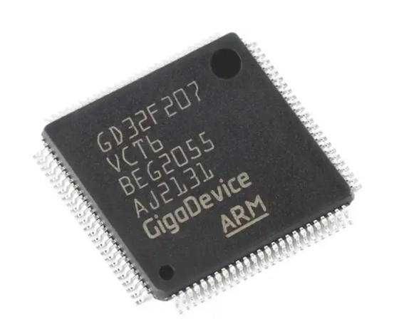

The Ultimate Guide to 8051 MCU Package: Types, Selection, and Applications
Introduction
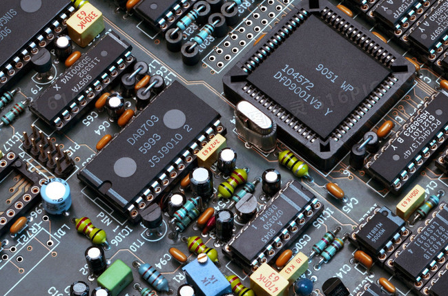
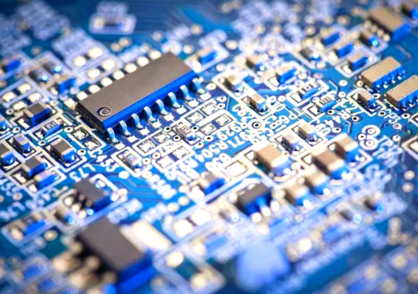
The 8051 microcontroller, introduced by Intel in 1980, has stood the test of time as one of the most influential and enduring architectures in the embedded systems world. While the core architecture has remained remarkably consistent over decades, the physical manifestation of these microcontrollers—their packages—has evolved significantly to meet changing technological demands. The 8051 MCU package is not merely a protective shell but a critical determinant of the microcontroller’s performance, thermal characteristics, and compatibility with target applications. Understanding package options is essential for engineers, designers, and procurement specialists working with this versatile microcontroller family. The diversity of available packages reflects the 8051’s adaptability to everything from simple consumer gadgets to sophisticated industrial systems. As we explore the landscape of 8051 packaging, we’ll uncover how this decades-old architecture continues to find relevance in modern electronics through appropriate packaging choices that balance form factor, cost, and functionality. Resources like ICGOODFIND can be invaluable for navigating the complex ecosystem of 8051 variants and their packaging options.
Understanding 8051 MCU Package Fundamentals
The Evolution of 8051 Packaging
The journey of 8051 MCU packaging began with conventional through-hole packages like PDIP (Plastic Dual In-line Package) that dominated the early years of microcontroller deployment. These packages featured lead pitches typically around 2.54mm (100 mils) and were designed for easy prototyping and manual assembly. As surface-mount technology gained prominence in the 1980s and 1990s, the 8051 family adapted with packages like PLCC (Plastic Leaded Chip Carrier) and SOIC (Small Outline Integrated Circuit) that offered reduced board space requirements and improved automated assembly characteristics. The relentless push toward miniaturization drove development of even more compact packages like TQFP (Thin Quad Flat Package) and QFN (Quad Flat No-leads) with lead pitches shrinking to 0.5mm and below. Modern 8051 derivatives now employ advanced packages such as BGA (Ball Grid Array) and WLCSP (Wafer-Level Chip-Scale Package) that maximize I/O density while minimizing footprint. This evolution reflects broader industry trends toward higher integration, better thermal performance, and increased reliability across temperature ranges and operating conditions.
Key Package Parameters and Their Significance
When evaluating 8051 MCU package options, several technical parameters demand careful consideration. Lead pitch—the distance between adjacent pins—directly impacts PCB design complexity and manufacturing requirements, with finer pitches necessitating more sophisticated fabrication and assembly capabilities. Package footprint determines the board real estate consumed, a critical factor in space-constrained applications. Thermal characteristics, including junction-to-ambient thermal resistance (θJA) and maximum operating temperature, influence power dissipation limits and cooling requirements. The number of available I/O pins varies significantly across packages, with larger packages typically offering more extensive peripheral connectivity. Material composition affects mechanical robustness, moisture sensitivity, and long-term reliability in harsh environments. Additionally, package height profile can be decisive in ultra-thin consumer products. Understanding these parameters enables informed trade-off decisions between size, cost, performance, and manufacturability when selecting 8051 variants for specific applications.
Comprehensive Overview of 8051 MCU Package Types
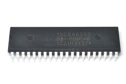
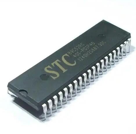
Through-Hole Packages
Through-hole packages represent the original packaging approach for 8051 microcontrollers and continue to serve important niches despite the industry’s shift toward surface-mount technology. The PDIP (Plastic Dual In-line Package) remains popular for prototyping, education, and low-volume production due to its hand-solderability and mechanical robustness. With typical lead counts ranging from 40 to 68 pins and a standard 2.54mm lead pitch, PDIP packages offer straightforward PCB layout with wide trace spacing. The CERDIP (Ceramic Dual In-line Package) variant provides enhanced thermal performance and hermetic sealing for military and aerospace applications where reliability under extreme conditions is paramount. Though through-hole technology has largely been superseded by surface-mount alternatives in mass production, these packages maintain relevance in applications requiring frequent manual insertion/removal, high mechanical stress tolerance, or where through-hole vias provide beneficial structural integrity. The continued availability of 8051 microcontrollers in through-hole packages demonstrates the architecture’s remarkable longevity and adaptability across generations of electronic manufacturing methodologies.
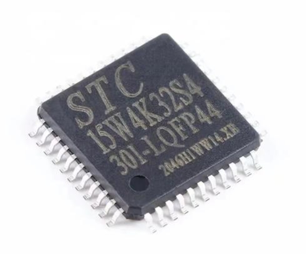
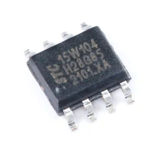
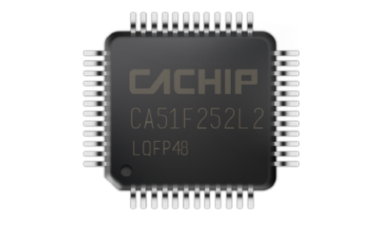
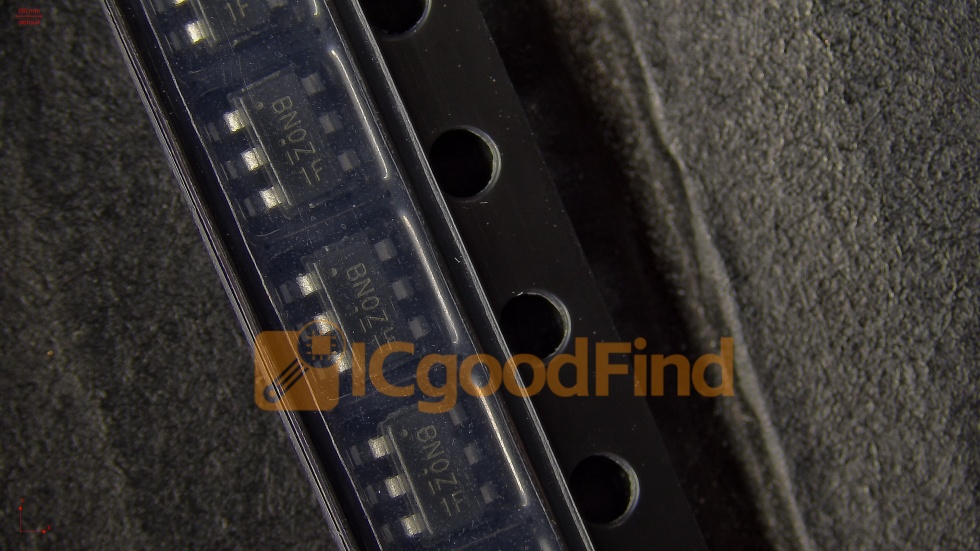
Surface-Mount Packages
Surface-mount packages dominate contemporary 8051 implementations, offering significant advantages in assembly automation, board space utilization, and high-frequency performance. SOIC (Small Outline Integrated Circuit) packages strike a balance between compactness and ease of handling, with lead pitches typically around 1.27mm (50 mils). The TQFP (Thin Quad Flat Package) has emerged as a workhorse for mid-range pin count applications (44 to 100+ pins), featuring a low profile (1.0mm height typical) and fine lead pitch (0.5mm or 0.8mm). For space-constrained designs, QFN (Quad Flat No-leads) packages provide exceptional thermal and electrical performance through exposed pads that facilitate direct heat sinking to the PCB, with some variants incorporating side-wettable flanks to enhance solder joint inspection. The progression toward miniaturization continues with WLCSP (Wafer-Level Chip-Scale Package) technology, where the package dimensions approximate the silicon die size itself, eliminating traditional interconnects to minimize parasitic effects while achieving the smallest possible form factor. Each surface-mount package type represents a specific point in the design trade-space between size, cost, thermal management, and manufacturability considerations.
Advanced and Specialized Packages
Beyond conventional packaging approaches, specialized 8051 variants employ advanced packaging technologies to address unique application requirements. BGA (Ball Grid Array) packages accommodate high pin counts (often exceeding 200 pins) while maintaining manageable overall dimensions through area-array interconnection rather than perimeter-only leads. This arrangement improves electrical performance through reduced inductance but complicates inspection and rework processes. For applications demanding minimal footprint without sacrificing I/O capability, CSP (Chip-Scale Package) implementations provide package sizes no more than 20% larger than the bare die while maintaining standard SMT compatibility. Some manufacturers offer system-in-package solutions that combine 8051 cores with complementary components like memory, RF transceivers, or sensors within a single package boundary. These heterogeneous integration approaches deliver functional completeness while simplifying overall system design. At the cutting edge, 3D packaging technologies enable stacking of multiple dies with through-silicon vias (TSVs) to create highly integrated subsystems with minimal interconnect length and enhanced performance characteristics.
Selecting the Right 8051 MCU Package for Your Application
Application-Specific Package Considerations
Choosing the optimal 8051 MCU package requires careful alignment with application constraints and performance requirements across several dimensions. For consumer electronics like wearables and IoT devices, miniature packages such as QFN and WLCSP dominate due to stringent size limitations and moderate thermal loads. These applications typically prioritize minimal footprint and low profile over maximum I/O count or power handling capability. Conversely, industrial automation systems often favor larger packages like LQFP (Low-profile Quad Flat Package) that accommodate extensive peripheral interfaces while providing robust mechanical characteristics suitable for harsh operating environments with vibration, humidity, and temperature extremes. The automotive sector imposes additional reliability standards that may dictate specialized qualification grades and packaging materials capable of withstanding extended temperature ranges (-40°C to +125°C or beyond) while maintaining signal integrity under electromagnetic interference. For medical devices, hermetic ceramic packages sometimes replace plastic alternatives to ensure long-term reliability in sterile environments or implantable applications where outgassing or moisture absorption could compromise functionality.
Manufacturing and Supply Chain Factors
Beyond technical specifications, practical considerations related to manufacturing capabilities and supply chain dynamics significantly influence 8051 MCU package selection decisions. Assembly facilities equipped primarily for conventional SMT processes may struggle with fine-pitch components below 0.5mm pitch or BGA packages requiring X-ray inspection capabilities. The availability of appropriate solder paste stencils, pick-and-place nozzles, and reflow profiling expertise should inform package choices early in the design cycle. From a supply chain perspective, certain package types enjoy broader manufacturer support and multiple sourcing options, reducing procurement risks compared to specialized or proprietary packaging approaches. Long-term availability considerations become particularly important for products with extended lifecycles spanning decades—a common scenario in industrial control and automotive applications where component obsolescence can necessitate costly redesigns. Additionally, thermal cycling reliability data should inform package selection for applications experiencing frequent power cycling or environmental temperature variations, as different package constructions exhibit varying resistance to solder joint fatigue over operational lifetime.
Conclusion
The remarkable longevity of the 8051 architecture owes much to its adaptable implementation across diverse package options that meet evolving market needs. From legacy through-hole formats maintaining compatibility with existing infrastructure to cutting-edge wafer-level chip-scale packages enabling tomorrow’s miniaturized devices, the 8051 MCU package ecosystem offers solutions spanning the entire spectrum of electronic product requirements. Successful implementation hinges on selecting package characteristics aligned with technical specifications, manufacturing capabilities, environmental constraints, and economic considerations specific to each application context. As packaging technology continues advancing with trends toward heterogeneous integration and 3D architectures, the venerable 8051 core finds new opportunities for deployment in increasingly sophisticated systems. Resources like ICGOODFIND provide valuable navigation through this complex landscape of options, helping engineers identify optimal pairings of silicon capability and physical implementation. The continued innovation in 8051 packaging ensures this foundational microcontroller architecture remains relevant in an ever-changing technological environment.