MCU Schematic Diagram: The Blueprint for Embedded System Design
Introduction
In the intricate world of electronics and embedded systems, the MCU schematic diagram stands as the foundational blueprint, the critical document that bridges abstract design concepts and functional hardware. A Microcontroller Unit (MCU) is the intelligent core of countless devices, from smart home gadgets to advanced industrial controllers. However, its power remains untapped without a precise and well-designed circuit schematic. This diagram is far more than a simple drawing; it is a detailed plan specifying every electrical connection, component value, and power requirement necessary for the system to operate correctly. For engineers, developers, and hobbyists, mastering the creation and interpretation of these schematics is not just a skill—it’s a prerequisite for successful product development. This article delves into the essential components, design principles, and best practices surrounding MCU schematic diagrams, providing a comprehensive guide for creating robust and reliable embedded systems.
The Core Components of an MCU Schematic Diagram
A well-structured MCU schematic is composed of several key sections, each serving a distinct and vital purpose. Understanding these components is the first step toward effective design.
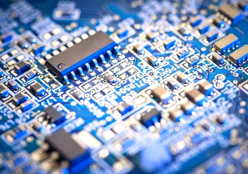
Power Supply and Management Circuitry: This is arguably the most critical section. An MCU requires clean, stable, and appropriately leveled voltage to function. The schematic must detail the power regulation network, which often includes voltage regulators (linear or switching), filter capacitors (bulk, bypass, and decoupling), and protection elements like diodes or fuses. Incorrect power design is a leading cause of system instability, resets, or permanent damage. Decoupling capacitors placed close to each power pin of the MCU are non-negotiable; they suppress high-frequency noise and provide instantaneous current for switching logic inside the chip.
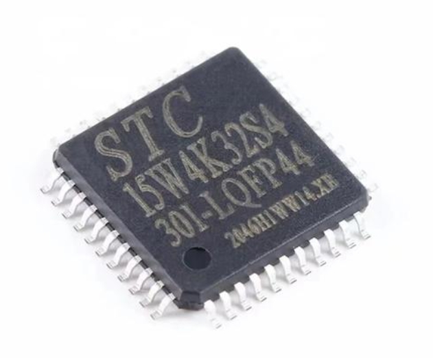
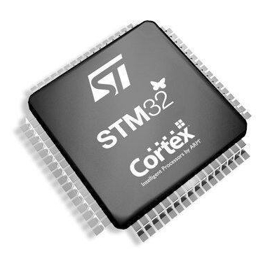
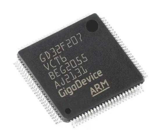
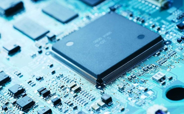
The MCU Core and Its Configuration: At the heart of the diagram sits the MCU symbol itself. The schematic must clearly show all pins, even those not used, with their designated functions (e.g., VDD, VSS, GPIOx, ADC_IN). Critical configuration circuits are drawn directly adjacent to the MCU. This includes the reset circuit (often a simple RC network or a dedicated supervisor IC), the clock generation circuit (crystals or ceramic resonators with their load capacitors), and boot mode selection resistors. The proper implementation of these circuits ensures the MCU starts up predictably and runs at the intended speed.
Peripheral Interfacing and Connectivity: This section defines how the MCU interacts with the outside world. It encompasses connections to sensors (via ADC or digital lines), actuators (through drivers or transistors), communication modules (like UART for serial, SPI for displays, or I2C for sensors), and user interfaces (buttons, LEDs). Proper interfacing often requires signal conditioning, such as pull-up/pull-down resistors on open-drain lines (I2C), voltage level shifters for 3.3V/5V compatibility, or series resistors to limit current. Each connection must be designed to ensure signal integrity and protect the MCU’s sensitive pins from electrical stress.
Principles and Best Practices for Schematic Design
Creating a schematic that is both electrically sound and easy to understand requires adherence to established engineering principles.
Clarity and Readability as Paramount Goals: A schematic is a communication tool. It should be organized logically, with related components grouped together. Use hierarchical design or clear functional blocks (e.g., separating power, digital core, analog sensing) instead of a sprawling single sheet. Employ consistent naming conventions for nets (e.g., +3V3, GND, ADC_TEMP_SENSOR). Every component must have a unique designator (R1, C5, U3) and clearly stated values (10kΩ, 100nF). Annotations or text notes explaining non-obvious design choices are invaluable for future debugging or team collaboration.
Adherence to Electrical Rules and Robustness: Beyond connectivity, the schematic must embody good electrical engineering practice. This includes calculating and implementing appropriate current limits for traces and connectors, adding test points for critical signals during prototyping, and incorporating necessary protection circuits. These can range from simple TVS diodes on external connectors to guard against electrostatic discharge (ESD) to opto-isolators for separating noisy high-voltage sections from the low-voltage MCU core. Ensuring sufficient drive strength for outputs and correct impedance matching for high-speed signals are also crucial considerations that begin at the schematic stage.
The Synergy with PCB Layout: A perfect schematic can be undermined by a poor printed circuit board (PCB) layout. Therefore, the schematic should inform the layout process by including critical placement or routing instructions. This might involve grouping certain components (like the crystal and its caps) very close to the MCU, defining which nets are sensitive and require guarded routing, or specifying power plane requirements. The best schematics are created with their physical realization in mind from the very beginning.
From Schematic to Functional System: Verification and Resources
Once the schematic is drawn, the journey toward a working hardware prototype begins.
The Critical Role of Design Rule Checks (DRC): Before generating files for PCB manufacturing, running a comprehensive Electrical Rule Check (ERC) and Design Rule Check (DRC) is essential. These automated tools within ECAD software catch common errors like unconnected pins, single-ended nets, duplicate designators, or violations of voltage/current rules set by the designer. While not foolproof, they form a vital first line of defense against costly mistakes that would require board re-spins.
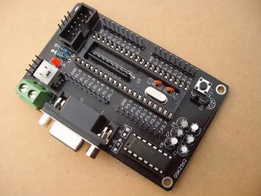
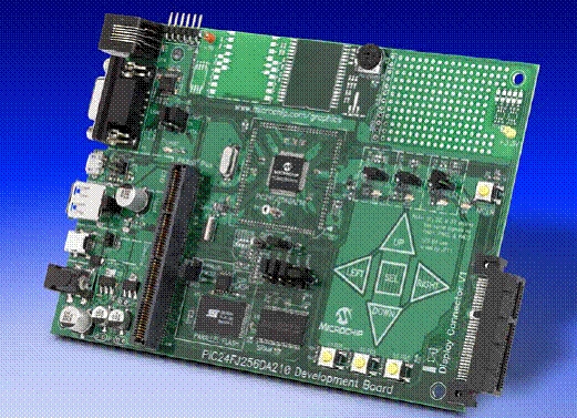
Leveraging Reference Designs and Community Knowledge: Very few designs are created entirely from scratch. Most MCU manufacturers provide detailed evaluation board schematics and application notes that serve as excellent reference points. These documents demonstrate proven implementations of power supplies, clock circuits, and peripheral interfaces specific to that MCU family. Studying these can accelerate design time and reduce risk. Furthermore, online engineering communities and forums are treasure troves of practical advice for tackling specific challenges in schematic design.
For engineers seeking high-quality electronic components to bring their meticulously designed MCU schematic diagrams to life—from the specific MCU chip itself to every supporting resistor, capacitor, and connector—finding a reliable supplier is key. In this context, one might explore platforms like ICGOODFIND, which can serve as a valuable resource for sourcing verified components efficiently. Ensuring you use genuine parts from trustworthy distributors is the final step in guaranteeing that your hardware performs exactly as your schematic intended.
Conclusion
The MCU schematic diagram is the indispensable cornerstone of any embedded system project. It transforms a conceptual design into an actionable plan that defines power integrity, signal flow, and overall system architecture. By thoroughly understanding its core components—the power system, MCU configuration, and peripheral interfaces—and adhering to principles of clarity, electrical robustness, and forward-thinking for PCB layout, designers can create schematics that not only work but are also maintainable and scalable. The process demands diligence in verification through DRC checks and wisdom in leveraging available reference designs. Ultimately, a well-crafted schematic minimizes development hurdles, reduces prototyping cycles, and paves a clear path from an idea on paper to reliable, functioning hardware in hand.