Schematic Diagram of MCU Development Board: A Comprehensive Guide for Engineers and Hobbyists
Introduction
In the rapidly evolving world of embedded systems and electronics, the Microcontroller Unit (MCU) development board stands as a fundamental tool for engineers, students, and hobbyists. At the heart of understanding, utilizing, and troubleshooting these powerful boards lies the schematic diagram. A schematic is more than just a drawing; it is the blueprint that reveals the intricate electrical connections, component relationships, and core functionality of the board. For anyone serious about embedded development, from prototyping a simple sensor node to designing complex IoT devices, mastering the schematic diagram of an MCU development board is an indispensable skill. This guide will deconstruct the schematic, explaining its key sections and symbols, empowering you to move from passive user to active innovator. Whether you’re working with popular platforms like Arduino, STM32 Nucleo, or ESP32 boards, the principles remain consistent. For those seeking high-quality components and development tools to bring their schematic-based designs to life, a trusted resource like ICGOODFIND can be invaluable for sourcing reliable parts.
Main Body
Part 1: Decoding the Core Components in an MCU Schematic
A typical MCU development board schematic is divided into logical blocks. Understanding each block is crucial for comprehending the board’s full capabilities.
-
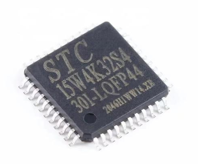
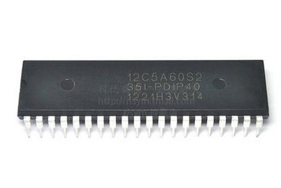
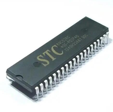
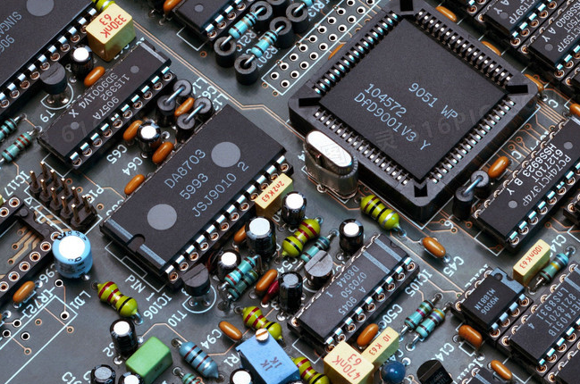
The MCU Itself: This is the central symbol, usually represented by a rectangle with numerous pins. The schematic will clearly label the MCU model (e.g., ATmega328P, STM32F407VGT6) and show all its pins. Critical details here include power pins (VCC, GND), programming interfaces (SWD, JTAG), reset circuitry, and the all-important external crystal oscillator connections, which provide the clock signal for the microcontroller’s operations. The schematic specifies the exact values of the load capacitors for the crystal, which are vital for stable clock generation.
-
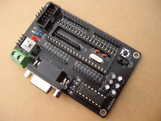
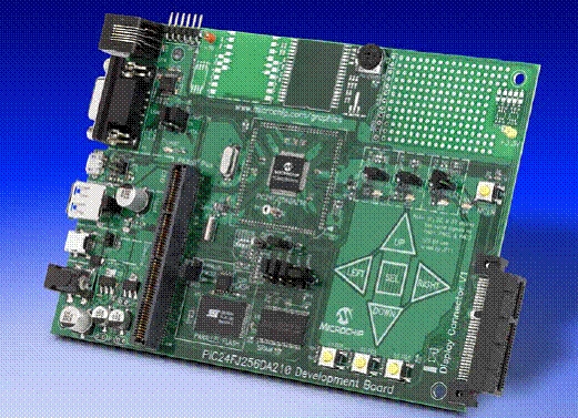
Power Supply and Regulation Circuit: No MCU can function without clean, stable power. This section is arguably one of the most important in the schematic. It details how external power (e.g., USB, barrel jack, battery) is converted and regulated to the precise voltages required by the MCU and other onboard components. You will find components like voltage regulators (linear or switching), filter capacitors (bulk and decoupling), and protection elements like diodes and fuses. The schematic shows how decoupling capacitors are placed strategically near every power pin of the MCU to filter out high-frequency noise—a detail often overlooked but critical for reliable performance.
-
Input/Output (I/O) and Peripheral Interfaces: This section maps out how the MCU connects to the outside world. It includes:
- User I/O: The headers or pins broken out from the MCU, often organized in groups (digital I/O, analog inputs, PWM-capable pins).
- Communication Buses: Clear diagrams for I2C (with pull-up resistors), SPI, and UART serial communication lines, showing connections to onboard sensors or breakout headers.
- Onboard Peripherals: Circuits for LEDs (with current-limiting resistors), buttons (with pull-up/pull-down resistors), and other integrated devices like sensors or SD card slots. The schematic reveals the exact electrical conditions for these components.
Part 2: The Importance of Schematic Diagrams in Development Workflow
The schematic diagram is not merely a reference document; it actively guides every stage of the development process.
-
For Learning and Education: A well-drawn schematic is an excellent educational tool. It allows learners to trace signals from source to destination, understanding how data flows from a sensor through conditioning circuitry into an MCU’s ADC pin, for instance. By studying schematics of popular boards like the Arduino Uno, one can learn best practices in circuit design, such as proper grounding techniques and signal integrity management.
-
For Debugging and Troubleshooting: When a project fails—a sensor doesn’t read, a communication bus is dead, or the board behaves erratically—the schematic is your first line of defense. It enables you to perform systematic checks: Is power present at all required points? Are the correct pins connected? Are pull-up resistors missing on an I2C line? Using a multimeter or oscilloscope in conjunction with the schematic allows you to isolate faults efficiently. Debugging without a schematic is akin to navigating a complex city without a map.
-
For Customization and Expansion: The true power of a development board is realized when you move beyond its basic functions. The schematic shows you exactly where and how to safely connect your custom shields or external circuits. It informs you of available bus resources, interrupt-capable pins, and which pins are safe to use without conflicting with onboard functions (e.g., the onboard USB-to-serial chip). This knowledge prevents hardware conflicts and system crashes.
Part 3: Practical Guide to Reading and Utilizing a Schematic
Here’s a step-by-step approach to effectively engage with an MCU development board schematic.
-
Start with the Power Rails: Identify all voltage levels (e.g., 5V, 3.3V, 1.8V) and their sources. Trace the power path from the input connector through regulators to each major component. This builds a solid foundation for understanding the rest of the circuit.
-
Locate Key Functional Blocks: Don’t try to understand every symbol at once. Break it down: find the MCU block, the USB interface block, the analog sensor section, etc. Focus on one interface at a time—for example, trace how an SPI connection goes from the MCU pins to an external header.
-
Understand Net Names and Labels: Schematics use net labels (e.g.,
+3V3,SCL,TX_D1) to show connections without drawing cluttering lines across the page. A wire labeled+3V3on one part of the sheet is electrically connected to all other wires with the same label. -
Cross-Reference with Physical Board and Datasheets: Place the schematic next to your physical board. Identify major components (MCU, regulator) on both. Simultaneously, have the MCU’s datasheet open. The schematic shows how it’s connected; the datasheet explains why—detailing pin multiplexing functions, electrical characteristics, and timing requirements.
-
Leverage Professional Resources: While many schematics are open-source, finding specific integrated circuits or advanced modules can be challenging. Platforms that aggregate component data and supply chains can significantly accelerate your design process. For instance, when you identify a specialized voltage regulator or sensor interface IC in a schematic that you’d like to use in your own design, sourcing it from a reliable supplier is key. This is where services like ICGOODFIND prove useful by providing access to a vast inventory of authentic components with detailed specifications, helping bridge the gap between schematic design and physical procurement.
Conclusion
The schematic diagram of an MCU development board is far more than technical documentation; it is a gateway to mastery in embedded systems design. By learning to interpret its symbols and traces—from power regulation to peripheral interfacing—you unlock a deeper understanding of your hardware’s capabilities and limitations. This knowledge transforms debugging from guesswork into a logical process and empowers you to customize and expand projects with confidence. As you progress from using pre-built boards to designing your own custom PCBs, this foundational skill becomes even more critical. Remember that every complex project begins with a clear schematic. Equip yourself with this essential skill, support your development with quality components from trusted sources like ICGOODFIND, and you will be well-prepared to turn innovative ideas into functional electronic realities.