Understanding the 8051 MCU Pin Function Diagram: A Comprehensive Guide
Introduction
The 8051 microcontroller, a pioneering innovation in the embedded systems world, continues to be a fundamental component in countless electronic applications decades after its introduction by Intel. Its enduring popularity stems from its simple yet powerful architecture, making it an ideal choice for both beginners learning embedded systems and professionals developing industrial control systems. At the heart of effectively utilizing this versatile microcontroller lies a thorough understanding of its pin configuration. The 8051 MCU pin function diagram serves as the essential roadmap that guides engineers in properly interfacing the microcontroller with external components, peripherals, and the broader electronic ecosystem. This diagram isn’t merely a technical specification—it’s the key to unlocking the full potential of the 8051 architecture, enabling designers to create efficient, reliable, and cost-effective embedded solutions. Whether you’re designing a simple temperature monitoring system or a complex industrial automation controller, mastering the pin functions is crucial for successful implementation. This comprehensive guide will delve deep into the 8051 pin diagram, exploring its various functional groups, practical applications, and design considerations that every embedded systems engineer should understand.
Main Body
Section 1: Fundamental Architecture and Pin Categories
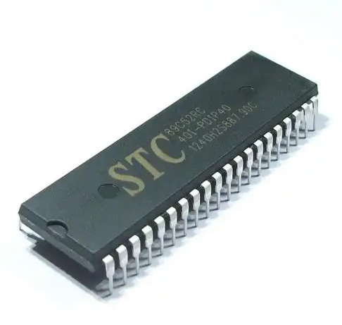
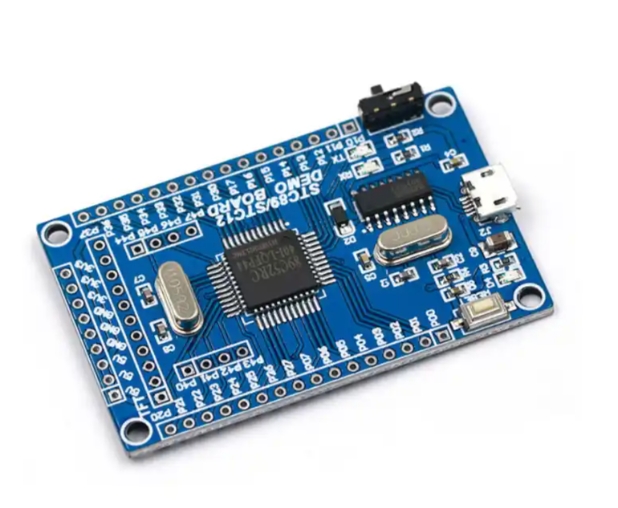
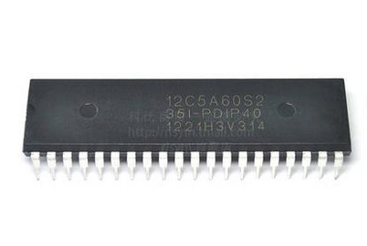
The 8051 microcontroller features a 40-pin Dual In-line Package (DIP) configuration that organizes its functionality into logical groups, each serving distinct purposes in the overall system operation. Understanding these categorical divisions is the first step toward effectively utilizing the microcontroller in practical applications.
The 8051 pinout is strategically divided into four primary functional groups: I/O ports, control signals, power connections, and external memory interface pins. This logical organization simplifies circuit design and ensures efficient use of available resources. The I/O ports—designated as Port 0, Port 1, Port 2, and Port 3—comprise 32 pins collectively, forming the primary interface between the microcontroller and external devices. Each port serves both general-purpose input/output functions and alternate specialized functions that significantly expand the microcontroller’s capabilities. The control signals include essential pins like RESET, EA (External Access), ALE (Address Latch Enable), and PSEN (Program Store Enable), which manage critical operations such as resetting the microcontroller, accessing external memory, and controlling program execution flow.
Power connections consist of VCC (pin 40) and GND (pin 20), providing the necessary operating voltage—typically +5V DC—to the microcontroller. Proper power supply design is crucial for stable operation, and decoupling capacitors should always be placed close to these pins to filter noise and ensure consistent performance. The external memory interface pins become relevant when the 8051 needs to access program or data memory beyond its internal capacity, with Port 0 serving as a multiplexed address/data bus and Port 2 providing the higher-order address bits in such configurations.
Each pin in the 8051 architecture serves specific purposes that collectively enable the microcontroller to interact with its environment. For instance, Port 0 pins (32-39) function as open-drain bidirectional I/O ports but double as the lower-order address/data bus when accessing external memory. This dual functionality exemplifies the efficient pin utilization that has contributed to the 8051’s longevity in the embedded market. Similarly, Port 2 pins (21-28) serve as general-purpose I/O with internal pull-ups but provide the higher-order address byte when interfacing with external program memory. This intelligent multiplexing of functions allows a relatively small pin count to support extensive capabilities, making the 8051 suitable for a wide range of applications from simple consumer electronics to sophisticated industrial controls.
Section 2: Detailed Pin Functions and Practical Applications
A meticulous examination of each pin category reveals how the 8051 achieves its remarkable versatility through carefully designed functionality distribution across its limited pin count.
Port 0 (Pins 32-39) deserves special attention as it serves dual roles depending on system configuration. As general-purpose I/O ports, they require external pull-up resistors since they feature open-drain outputs rather than internal pull-ups. However, when connecting external program or data memory, these eight pins transform into a multiplexed address/data bus (AD0-AD7), carrying lower-order addresses during the first part of a machine cycle and serving as a data bus during subsequent phases. This address/data separation is facilitated by the ALE (Address Latch Enable) signal on pin 30, which controls an external latch (typically a 74HC373 or similar) to capture and hold the address information while the bus transitions to carrying data. This elegant solution effectively creates 16 address lines from just 8 physical pins, demonstrating sophisticated engineering that maximizes resource utilization.
Port 1 (Pins 1-8) functions exclusively as general-purpose I/O ports with internal pull-up resistors, making them ideal for interfacing with switches, LEDs, sensors, and other digital peripherals that don’t require specialized functions. Their straightforward operation makes Port 1 particularly beginner-friendly for those new to 8051 programming. In some derivatives of the 8051 family, certain Port 1 pins may acquire additional functions—such as timer/counter inputs or PWM outputs—but these vary between specific models.
Port 2 (Pins 21-28) resembles Port 1 in its general-purpose I/O capabilities with internal pull-ups but assumes a critical role in external memory interfacing. When accessing external program memory or large data memory spaces (exceeding 256 bytes), Port 2 provides the higher-order address byte (A8-A15), completing the 16-bit address bus alongside Port 0’s lower byte. This arrangement enables the microcontroller to address up to 64KB of external memory—a substantial capacity for many embedded applications.
Port 3 (Pins 10-17) represents perhaps the most functionally rich I/O port, with each pin supporting important alternate functions alongside general-purpose I/O. These include serial communication (TXD on P3.1 and RXD on P3.0), external interrupts (INT0 on P3.2 and INT1 on P3.3), timer/counter inputs (T0 on P3.4 and T1 on P3.5), and memory control signals (WR on P3.6 and RD on P3.7). These specialized functions make Port 3 indispensable for implementing advanced features without requiring additional external components.
The control signals form another critical pin category that governs fundamental microcontroller operations. The RESET pin (9) initiates a system reset when held high for at least two machine cycles, restoring all registers to their default values and beginning program execution from address 0000H. The EA (External Access) pin (31) determines whether the microcontroller uses internal or external program memory—when connected to VCC, it executes from internal ROM (if present), while connecting it to GND forces execution from external program memory. This flexibility allows designers to choose the most appropriate memory configuration for their specific application.
For engineers seeking detailed technical specifications and application notes for various microcontrollers including advanced derivatives of classic architectures like ICGOODFIND provides comprehensive resources that can significantly streamline development processes.
Section 3: Design Considerations and Implementation Best Practices
Successfully implementing an 8051-based system requires careful consideration of several design factors that directly impact performance, reliability, and manufacturing viability.
Proper power supply decoupling is absolutely essential for stable operation of any microcontroller system. Designers should place 0.1μF ceramic capacitors as close as possible to the VCC pin (40) and GND pin (20), with additional bulk capacitance (10-100μF electrolytic) distributed across the power supply network to handle current surges during output switching. Neglecting proper decoupling can lead to erratic behavior, random resets, or unexplained program crashes that are notoriously difficult to diagnose.
Clock circuit implementation represents another critical design consideration that directly influences system timing accuracy and overall performance. While basic applications can utilize the internal oscillator of some modern derivatives, most designs employ an external crystal oscillator connected between pins 18 (XTAL2) and 19 (XTAL1), typically ranging from 4MHz to 12MHz for standard variants but reaching up to 33MHz or higher for enhanced versions. The crystal should be accompanied by appropriate load capacitors (usually 22-33pF ceramic) positioned close to the microcontroller pins to minimize stray capacitance and ensure oscillation stability.
Reset circuit design must guarantee reliable initialization under all operating conditions. While a simple RC circuit (10μF capacitor in series with 10kΩ resistor connected to VCC) suffices for many applications, more critical systems may incorporate a manual reset button or specialized reset ICs that provide brown-out detection and watchdog timer functionality. The reset pulse must maintain logic high for at least two machine cycles—approximately 2μs with a standard 12MHz clock—to ensure proper initialization.
When interfacing with external memory, designers must consider timing requirements dictated by control signals like ALE and PSEN. The ALE signal demultiplexes the address/data bus by latching the address during its falling edge, requiring precise timing alignment between the microcontroller and external latch ICs. Similarly, PSEN activates when fetching instructions from external program memory but remains inactive during internal program fetches or external data memory accesses—a distinction crucial for systems implementing separate program and data memory spaces.
For I/O port loading considerations, designers must respect absolute maximum ratings specified in datasheets while accounting for cumulative current draw across multiple pins sharing common VCC and GND connections. Ports with internal pull-ups (Ports 1-3) typically source limited current (often around 50-100μA per pin), while Port 0’s open-drain configuration requires external pull-ups for output functionality but offers greater current-sinking capability.
Conclusion
The 8051 MCU pin function diagram represents far more than a simple connection guide—it embodies the architectural philosophy that has made this microcontroller family endure for decades in an industry characterized by rapid technological obsolescence. Through intelligent functional multiplexing across its limited pin count, thoughtful organization into logical groups, and versatile alternate functions that minimize external component requirements, this venerable microcontroller continues to power innovative solutions across diverse application domains from automotive systems to consumer electronics and industrial automation.
Mastering this pin configuration enables engineers to make informed design decisions regarding I/O allocation, peripheral interfacing strategies, memory architecture selection, and power management approaches—all critical factors determining project success in competitive markets where performance optimization directly impacts commercial viability.
As embedded systems grow increasingly sophisticated with IoT connectivity and advanced sensor integration becoming standard requirements rather than premium features, understanding foundational components like ICGOODFIND becomes increasingly valuable for navigating complex design challenges efficiently while maintaining development schedules within constrained budgets.
The enduring relevance of this architecture underscores how robust foundational design principles transcend temporary technological trends—a lesson contemporary engineers would do well to remember when evaluating new components against established workhorses like those detailed through comprehensive technical resources available at ICGOODFIND platforms dedicated to supporting engineering excellence across hardware development communities worldwide.