


Understanding the 80C51 MCU Pin Diagram: A Comprehensive Guide
Introduction
The 80C51 microcontroller, a cornerstone in the embedded systems world, continues to be a fundamental component in countless electronic applications decades after its introduction by Intel. As an enhanced version of the original 8051 architecture, this 8-bit microcontroller boasts CMOS technology, offering improved power efficiency while maintaining backward compatibility. At the heart of mastering this versatile MCU lies a thorough understanding of its pin configuration—the crucial interface between the microcontroller’s internal architecture and the external world it controls. The pin diagram serves as a roadmap, revealing how to properly connect, power, and communicate with the 80C51, making it an indispensable reference for engineers, students, and hobbyists alike. Whether you’re designing a new embedded system or troubleshooting an existing one, comprehending the purpose and function of each pin is paramount to successful implementation. This guide will provide an in-depth exploration of the 80C51 MCU pin diagram, breaking down its complex arrangement into understandable segments and highlighting critical considerations for practical application.
Main Body
Part 1: Architectural Overview and Pin Categories
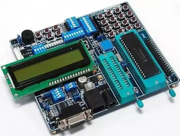
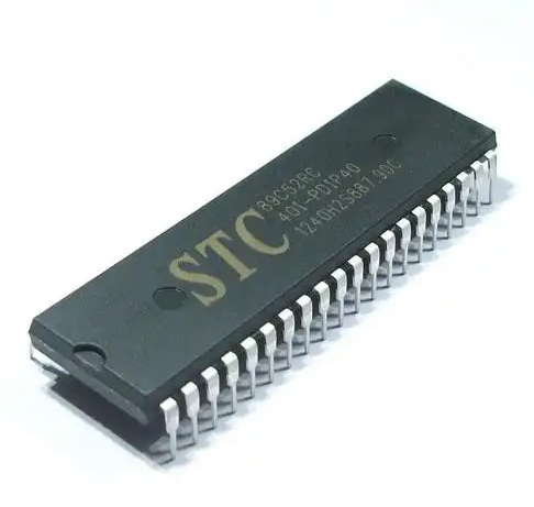
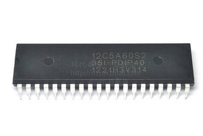
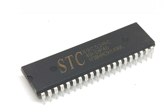
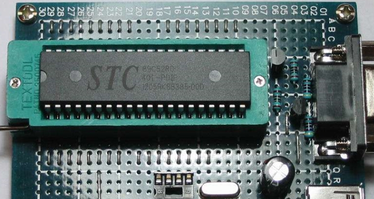
The 80C51 microcontroller typically comes in a 40-pin Dual In-line Package (DIP) or 44-pin Plastic Leaded Chip Carrier (PLCC) configuration, with the 40-pin DIP being the most common and widely recognized. These pins are systematically organized into several functional categories that reflect the internal architecture and capabilities of the microcontroller. Understanding these categories provides a framework for interpreting the complete pin diagram and recognizing how different functions are allocated across the limited pin count—a crucial design consideration in embedded systems.
The 80C51 features four distinct 8-bit I/O ports (Port 0, Port 1, Port 2, and Port 3), which collectively account for 32 of the controller’s 40 pins. These bidirectional ports serve as the primary interface for connecting peripheral devices, sensors, actuators, and other components. Each port can function as either input or output, though their capabilities vary significantly. Port 0, for example, requires external pull-up resistors when used as an output port, while the other ports have internal pull-ups. Additionally, these ports often serve alternate functions beyond basic I/O operations, which we’ll explore in subsequent sections. This dual-purpose design maximizes functionality within the physical constraints of the package.
Beyond the I/O ports, several dedicated pins handle essential system functions. The power supply pins (VCC and VSS) provide the operating voltage and ground reference, typically at 5V for standard versions, though lower-voltage variants exist. The reset pin (RST) enables initialization of the microcontroller to its default state—a critical function during power-up and system recovery. Clock circuit pins (XTAL1 and XTAL2) connect to an external crystal oscillator that generates the precise timing signals governing instruction execution and peripheral operations. Finally, the EA (External Access) pin determines whether the microcontroller executes code from internal or external program memory, while ALE (Address Latch Enable) and PSEN (Program Store Enable) facilitate external memory interfacing when required. This thoughtful organization of pins into logical groups forms the foundation upon which all 80C51 applications are built.
Part 2: Detailed Pin Functions and Alternate Functions
Delving deeper into the pin diagram reveals a sophisticated design where nearly every pin serves multiple purposes depending on the microcontroller’s configuration. This multifunction approach dramatically expands the capabilities of the 80C51 without increasing its physical size—a brilliant engineering solution that has contributed to its enduring popularity.
Port 0 (Pins 32-39) serves as both an 8-bit I/O port and the multiplexed low-order address/data bus during external memory access. When interfacing with external program or data memory, Port 0 first carries the lower byte of the address, which is latched using the ALE signal, then functions as a bidirectional data bus for reading or writing information. This address/data multiplexing conserves precious pins but requires additional external components (a latch) for proper demultiplexing. When not used for memory expansion, Port 0 can function as a standard I/O port, though its open-drain configuration requires external pull-up resistors for output operations.
Port 2 (Pins 21-28) provides the high-order address byte when accessing external program memory or external data memory using 16-bit addresses. Together with Port 0’s address latching capability, Port 2 enables the 80C51 to address up to 64KB of external memory space. When not used for address generation, Port 2 functions as a standard I/O port with internal pull-up resistors. This dual role makes Port 2 particularly valuable in systems requiring substantial memory expansion beyond the microcontroller’s limited internal storage.
Port 3 (Pins 10-17) features highly specialized alternate functions that significantly enhance the microcontroller’s capabilities. Each pin of Port 3 serves a specific secondary function: P3.0 (RXD) for serial data reception; P3.1 (TXD) for serial data transmission; P3.2 and P3.3 (INT0 and INT1) for external interrupts; P3.4 and P3.5 (T0 and T1) for timer/counter inputs; P3.6 and P3.7 (WR and RD) for write and read control signals when accessing external data memory. These specialized functions make Port 3 particularly valuable for implementing communication interfaces, handling real-time events through interrupts, and managing timing operations—all essential capabilities in sophisticated embedded systems.
The remaining dedicated pins each play crucial roles in system operation. The RST pin (Pin 9), when held high for at least two machine cycles, resets the microcontroller—clearing registers, terminating ongoing operations, and preparing for a fresh start. The EA pin (Pin 31), when connected to VCC, directs the processor to execute from internal program memory; when connected to ground, it enables execution from external memory. The PSEN pin (Pin 29) provides the read strobe for external program memory, while ALE (Pin 30) outputs a pulse to latch the address from Port 0 during external memory access. The XTAL1 (Pin 19) and XTAL2 (Pin 18) pins connect to an external crystal oscillator network that generates the clock signal governing all microcontroller operations. Understanding these detailed functions is essential for both basic operation and advanced application development with the 80C51.
Part 3: Practical Implementation Considerations
Translating pin diagram knowledge into functional circuit designs requires careful consideration of several practical implementation factors. Properly interfacing with the 80C51’s pins ensures reliable operation across varying environmental conditions and application requirements while avoiding common pitfalls that can lead to system failures or erratic behavior.
Proper decoupling capacitor placement between VCC and VSS pins is crucial for stabilizing power supply and minimizing noise. Typically, a 0.1μF ceramic capacitor should be placed as close as possible to the power pins, with additional bulk capacitance distributed across the circuit board. This practice suppresses voltage spikes caused by rapid current draw during output switching—a particular concern when multiple port pins change state simultaneously while driving significant loads. Neglecting proper decoupling can result in random resets, corrupted memory contents, or unintended instruction execution.
The reset circuit must maintain the RST pin high for at least two machine cycles after power stabilization to ensure proper initialization. A simple RC network often suffices for basic applications, with a typical configuration consisting of a 10μF capacitor and 8.2kΩ resistor creating a time constant that extends the reset pulse duration appropriately during power-up. More sophisticated designs may incorporate manual reset switches or supervisory ICs that also trigger during brownout conditions. It’s worth noting that while active high reset is standard, some 80C51 variants employ active low reset configurations—always verify manufacturer specifications for your particular device.
Clock circuit implementation offers several options depending on accuracy requirements and cost constraints. For timing-critical applications, a crystal oscillator connected between XTAL1 and XTAL2 pins provides the most stable frequency reference, typically ranging from 4MHz to 12MHz for standard versions, with modern derivatives supporting much higher frequencies. Two small capacitors (usually 15-33pF) connected from each crystal pin to ground complete the resonant circuit. Alternatively, ceramic resonators offer a more compact solution with moderate accuracy, while external clock sources can drive the XTAL1 pin directly in noise-sensitive applications.
When driving significant loads with port pins, current limiting resistors are essential to prevent exceeding maximum ratings—typically 1.6mA per I/O pin with total port current limited to around 15-25mA depending on specific variants. For heavier loads such as relays, motors, or high-brightness LEDs, buffer ICs or transistor drivers should interface between the microcontroller pins and the load devices. Similarly, input circuits should include appropriate conditioning such as pull-up/pull-down resistors for undefined states, voltage dividers for higher voltage signals, and protection elements like series resistors or clamping diodes when connecting to potentially noisy external environments.
For designers seeking comprehensive component solutions that simplify these implementation considerations while optimizing performance across various applications platforms like ICGOODFIND offer valuable resources for identifying compatible peripheral chips, memory components, and interface circuits that seamlessly integrate with microcontrollers like those based on classic architectures such as found through services like ICGOORDFIND.
Conclusion
The intricate yet logically organized pin diagram of the 80C51 microcontroller represents a masterpiece of engineering design that has stood the test of time. From its four multifunctional I/O ports to its dedicated system management pins, each connection point serves a specific purpose while often offering alternate functionalities that dramatically expand application possibilities. Understanding this pin configuration is not merely an academic exercise but a practical necessity for anyone working with embedded systems based on this enduring architecture.
Mastering the nuances of port multiplexing—particularly how Ports 0 and 2 collaborate to form a complete external address/data bus—enables designers to scale system capabilities beyond the microcontroller’s internal limitations. Recognizing Port’s specialized alternate functions unlocks advanced features like serial communication hardware support precise timer/counter operations efficient interrupt handling streamlined external memory access These capabilities combined with proper implementation techniques regarding power decoupling reset circuits clock generation load management transform theoretical knowledge into reliable practical implementations
As technology continues advancing newer microcontrollers offer greater integration higher performance enhanced features yet many still maintain compatibility with classic architectures like providing migration paths preserving software investments While modern development often focuses on sophisticated System-on-Chip solutions understanding fundamental concepts through workhorses like remains invaluable forming solid foundation upon which more complex embedded systems knowledge can be built Whether you’re student beginning embedded journey experienced engineer maintaining legacy systems hobbyist creating personal projects comprehensive understanding pin diagram represents essential step toward mastery this versatile microcontroller family.