Understanding the 8051 Microcontroller Pin Diagram: A Comprehensive Guide
Introduction
The 8051 microcontroller stands as one of the most influential and enduring architectures in the embedded systems world. Since its introduction by Intel in 1980, this 8-bit MCU has powered countless devices across industrial, automotive, consumer electronics, and educational applications. What makes the 8051 particularly remarkable is its elegant balance of simplicity and capability—a design philosophy that continues to resonate with engineers decades after its creation. At the heart of understanding and effectively implementing this microcontroller lies a thorough comprehension of its pin configuration and functionality. The pin diagram serves as the fundamental roadmap that connects the internal architecture of the 8051 to the external world, enabling designers to interface with sensors, actuators, displays, communication modules, and numerous other peripheral devices.
For engineers, students, and hobbyists working with embedded systems, mastering the 8051 pin diagram is not merely an academic exercise but a practical necessity for successful project implementation. Each pin on the 8051 package represents a specific function or capability that, when properly understood and utilized, unlocks the full potential of this versatile microcontroller. Whether you’re designing a basic input/output system or a complex embedded application, the pin diagram provides the critical interface between your software code and physical hardware components. This guide will explore the 8051 pin configuration in exhaustive detail, examining the purpose and operation of each pin group while providing practical implementation insights that bridge theoretical knowledge with real-world application.

Part 1: Overview of 8051 Microcontroller Pin Configuration
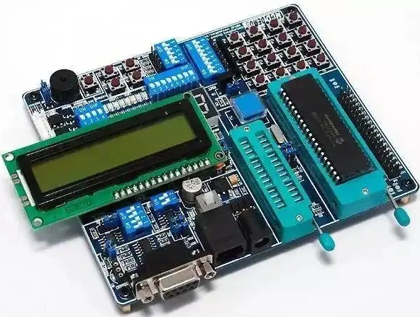
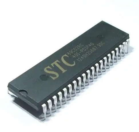
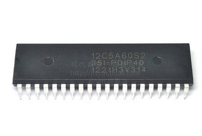
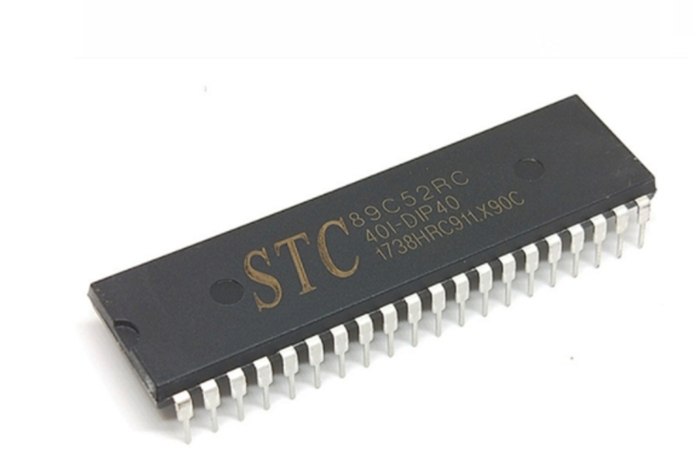
The standard 8051 microcontroller is typically available in a 40-pin Dual In-line Package (DIP) configuration, though surface-mount variants with different pin counts also exist. These 40 pins are systematically organized into four distinct ports (Port 0, Port 1, Port 2, and Port 3), along with dedicated pins for power supply, reset circuitry, clock generation, and external memory interfacing. This logical grouping reflects the microcontroller’s internal architecture and provides a structured approach to understanding how the 8051 communicates with external components.
The physical arrangement of pins follows a consistent numbering convention, with Pin 1 typically identified by a small dot or notch on the packaging. Pins are numbered counter-clockwise from this reference point, with pins 1-20 on one side and pins 21-40 on the opposite side of the DIP package. This standardized physical layout ensures compatibility across different manufacturers and simplifies the PCB design process. It’s worth noting that while the physical arrangement remains consistent, not all 8051 variants utilize every pin—some specialized versions may omit certain features or repurpose pins for application-specific functions.
Understanding the pin diagram requires recognizing that most pins serve multiple functions depending on the microcontroller’s configuration. This multiplexing capability is one of the 8051’s most powerful features, allowing a limited number of pins to support an extensive range of operations. For example, many I/O port pins double as data/address lines for external memory access or as control signals for special functions. This functional flexibility comes with complexity, however, as designers must carefully manage these alternate functions through proper configuration of internal registers and external circuitry.
The importance of proper pin understanding extends beyond mere connection correctness. Signal integrity, timing considerations, and electrical characteristics all play crucial roles in system reliability. Designers must account for factors such as sink/source current limitations, voltage thresholds, capacitive loading, and noise immunity when interfacing with external devices. Furthermore, understanding the reset and clock circuitry requirements is essential for establishing stable operation from power-up through normal execution. These foundational aspects collectively determine whether an 8051-based system will function reliably in its intended environment.
Part 2: Detailed Analysis of Pin Functions and Groups
Power Supply Pins (VCC and GND)
The 8051 requires a single +5V DC power supply connected between VCC (Pin 40) and GND (Pin 20). This straightforward power requirement contributed significantly to the microcontroller’s popularity, as it aligned with the dominant logic voltage levels of its era. Proper power supply design is critical for stable operation—the 8051 typically consumes between 10-50mA during normal operation, though this varies based on clock frequency and activated peripherals. Decoupling capacitors placed close to the power pins are essential for filtering high-frequency noise and maintaining voltage stability during rapid current transitions. While modern microcontrollers often feature multiple power domains and lower operating voltages, the 8051’s simple single-voltage scheme remains one of its most accessible characteristics for beginners.
Reset Circuitry (RST)
Pin 9 serves as the active-high Reset input for the 8051 microcontroller. A high pulse lasting at least two machine cycles (typically 24 clock cycles) on this pin forces the microcontroller into a known initial state—the Program Counter resets to 0000H, all ports assume their default states, and special function registers return to their initial values. The simplest reset circuit consists of a capacitor connected between VCC and the RST pin, with a resistor connecting RST to GND. This RC network creates an automatic power-on reset while also supporting manual reset via a push-button switch. More sophisticated designs often incorporate reset supervisor ICs that provide reliable operation across varying power conditions. Proper reset circuit design is non-negotiable for production systems, as it ensures consistent startup behavior regardless of power supply characteristics or environmental factors.
Clock Circuitry (XTAL1 and XTAL2)
The 8051 incorporates an on-chip oscillator that requires an external timing reference connected between XTAL1 (Pin 19) and XTAL2 (Pin 18). This typically takes the form of a quartz crystal or ceramic resonator spanning these two pins, with appropriate load capacitors completing the resonant circuit. The clock frequency fundamentally determines instruction execution speed—each machine cycle consumes 12 clock periods, with most instructions requiring one or two machine cycles. While the original 8051 operated at up to 12MHz, modern derivatives often support frequencies exceeding 30MHz. Alternatively, an external clock source can drive XTAL1 directly while leaving XTAL2 unconnected. Clock stability directly impacts timing-critical operations like serial communication baud rate generation and hardware timer accuracy, making proper oscillator design essential for reliable system performance.
Input/Output Ports (Ports 0-3)
The four 8-bit I/O ports represent the 8051’s primary interface with external devices:
Port 0 (Pins 32-39) serves dual functions as either general-purpose I/O or as the multiplexed lower address byte (A0-A7) and data bus (D0-D7) when interfacing with external memory. As I/O, these pins operate in open-drain mode requiring external pull-up resistors for output high signals. During external memory access, Port 0 automatically switches to its multiplexed address/data function, eliminating the need for software configuration.
Port 1 (Pins 1-8) functions exclusively as general-purpose I/O with internal pull-ups. These pins provide straightforward digital input/output capability without alternate functions on the basic 8051 architecture. Later derivatives have assigned special functions to certain Port 1 pins (such as ADC inputs or PWM outputs), but these implementations vary by manufacturer.
Port 2 (Pins 21-28) operates either as general-purpose I/O or supplies the upper address byte (A8-A15) during external memory accesses that use all 16 address lines. Unlike Port 0’s multiplexed operation, Port 2 dedicates its entire byte exclusively to address output when accessing external program memory or16-bit addressed data memory.
Port 3 (Pins 10-17) features general-purpose I/O capabilities alongside critically important alternate functions that significantly expand the microcontroller’s connectivity options: - P3.0 (Pin 10): RXD - Serial data input - P3.1 (Pin 11): TXD - Serial data output - P3.2 (Pin 12): INT0 - External interrupt 0 - P3.3 (Pin 13): INT1 - External interrupt 1 - P3.4 (Pin 14): T0 - Timer/Counter 0 external input - P3.5 (Pin 15): T1 - Timer/Counter 1 external input - P3.6 (Pin 16): WR - External data memory write strobe - P3.7 (Pin 17): RD - External data memory read strobe
These alternate functions make Port 3 particularly valuable for system expansion, providing essential communication interfaces without requiring external components.
External Memory Control Signals
When an application requires more memory than the onboard ROM or RAM, the EA (External Access), PSEN (Program Store Enable), and ALE (Address Latch Enable) pins manage communication with external memory devices:
EA (Pin 31) determines whether the microcontroller executes code from internal or external program memory. Tying this pin high (to VCC) causes program execution to begin from internal ROM addresses (0000H-0FFFH for the basic 8051), while pulling it low forces execution entirely from external memory. This flexibility allows designers to choose between cost-optimized internal execution and expanded capability through external memory.
PSEN (Pin 29) provides the read strobe for external program memory fetch operations. This output signal activates when the program counter addresses locations beyond the internal ROM capacity or when EA is held low. PSEN remains inactive during internal program fetches or external data memory accesses.
ALE (Pin 30) outputs a pulse during each machine cycle to demultiplex the address/data bus on Port 0. When using external memory, the lower address byte appears briefly on Port 0 before transitioning to data bus operation—an external latch captures this address using ALE as its enable signal. ALE also runs at 1/6th the oscillator frequency when no memory access occurs, potentially serving as a system clock reference.
Part III: Practical Implementation Considerations
Interfacing Techniques and Circuit Design
Successfully implementing an 8051-based system requires more than just understanding pin functions—it demands thoughtful circuit design that accounts for electrical characteristics and real-world operating conditions. Each I/O port exhibits different drive capabilities and electrical behaviors that significantly impact interface design. Ports 1,2, and3 feature internal pull-up resistors approximately30kΩ in value,sourcing limited current(typically50-100μA).Port0lacks these pull-ups in output mode,making it suitable primarily for driving low-power loads or when used with external pull-up resistors.For higher current requirements such as driving LEDs or relays,buffer ICs like74HC245or discrete transistors become necessary additions.
When designing input circuits,proper consideration of logic level thresholds ensures reliable signal detection.The8051recognizes voltages below1.2Vas logic lowand above2.4Vas logic highwith maximum ratingsof2.0Vfor VIHand0.8Vfor VIL.Noise immunity improves significantly when signals swing fully between rail voltages.Floating inputs should be avoided through pull-up or pull-down resistors as they increase power consumptionand may cause unpredictable behavior.Schmitt-trigger inputs available on some derivatives provide enhanced noise rejection for slowly changing or noisy signals.
Memory Expansion Strategies
The8051’s64KBexternal memory address space(separatelyforprogramanddata)enables substantial system expansion when onboard resources prove insufficient.Properly implementing external memory requires careful coordination of multiple pin functions.TheALE signal latches the lower address byte from Port0into an external register(typically74HC373or similar)while Port2provides the upper address byte.The same Port0pins then serve as the bidirectional data bus during read/write operations.This address/data multiplexing conserves pins but adds complexity through required support components.
Program memory expansion utilizesPSENas thereadstrobe while data memory accesses employRDandWRsignalsfromPort3.This Harvard architecture separation allows simultaneous connectionto separate programanddata memory devices.Designers must consider timing parameters—particularly address validto data valid delaysandhold times—when selecting memory components.Many modern applications instead utilize bank switching techniques or serial peripheral memories like SPI FLASH to conserve pins while still expanding storage capability.
Special Function Utilization
Beyond basic digital I/O,the8051pins provide access to integrated peripherals that dramatically reduce system component count.The serial communication capabilities available through P3.0andP3.1enable UART connectivitywith minimal external components—typically just level shifters like MAX232for RS-232compatibility or direct connection to other logic devices.Baud rate generation derives from Timer1configured in auto-reload mode,making accurate frequency selection straightforward through proper timer initialization.
The external interrupts on P3.2andP3.support either level-activated or edge-triggered operation selected through configuration bits in the TCON register.These interrupts provide rapid response to external eventswithout polling overhead,making them ideal for time-critical inputs like emergency stopsorzero-crossingdetection.Similarly,the timer/counter inputs on P3andP3allowexternal event countingorfrequency measurementby configuringthe timersin appropriate modes.
Configuration Management Best Practices
Effectively managingthe8051pin configurationsrequires understandinghowsoftware decisionsimpact hardware functionality.Port initialization occurs automatically at resetbutcan be modifiedduring programexecution.Writingtoaport latch registerestablishesoutput valueswhile readingreturns eitherthe latchstateorthe actualpinvoltage dependingon whetherthe portis configuredfor outputorinput.The alternatefunctions ofPorts0,,and3are controlledthrough specificregisteroperationsormemoryaccessesthat automaticallyoverridegeneral-purposeI/Obehavior.
Designersshould developconsistentstrategiesfor managingtheseconfigurationsacrosstheapplication.For example,routines thattemporarilyusePortfor general-purposeI/Owhileexternalmemoryis notbeing accessedmustrestoretheporttoitsmultiplexedmodepriortoany subsequentmemoryoperations.Similarly,theserialportalternatefunctionstake precedenceovergeneral-purposeI/O,makingsharedpinusage challengingwithoutcarefulprotocol design.Documentingtheseinteractionswithcommentaryin sourcecodehelps preventconfigurationconflictsduringmaintenanceordevelopment.
Conclusion
The enduring relevanceofthe805microcontrollerstemsnotjustfromitsarchitecturalelegancebutfromthedeliberatedesignofitspininterface thatbalancescapabilitywithaccessibility.Masteringthepindiagramtranscendsmemorization—itrepresentsunderstandinghowtobridgetheabstractworldofsoftwarewiththephysicalworldofelectroniccircuits.Eachpin group serves specificpurposeswhilemaintainingflexibilitythroughcarefullyplannedmultiplexingarrangements.Fromthefundamentalpowersupplyconnectionstothesophisticatedexternalmemoryinterface,thepinscollectivelyenablethevastapplicationrangelthat hasmadethe805aperennialchoiceforembeddedsystems.
For engineers seeking comprehensive resources on microcontrollersystemdesign,ICGOODFIND offers extensive reference materials,componentselectionguides,andpracticalimplementationexamplesspanningfrombasicinterfacingtocomplexsystemintegration.Theircuratedtechnicalcontentprovidesvaluablecontextforapplyingtheoreticalknowledgetoreal-worlddesignchallengesacrossvariedapplicationscenarios.Whetherworkingwithlegacy805derivativesormodernenhancedversions,thedetailedpinknowledgepresentedinthisguideformsthefoundationforsuccessfulembeddeddevelopment.
As technology continues evolving,the fundamental principles embodied inthe805pinconfigurationremainrelevant—clearlydefinedinterfaces,sensiblemultiplexingstrategies,andconsistentelectricalcharacterizationcontinuetoguidecontemporarymicrocontrollerdesigns.Thedepthofunderstandinggainedfromstudyingthisclassicarchitectureprovidesenduringvaluethattranscendsspecificimplementationdetails,makingthetimelesseducationalinvestmentforengineersatall experiencelevels.