


Demystifying the Machine Cycle of the 8051 MCU: The Heartbeat of an Embedded Legend
Introduction
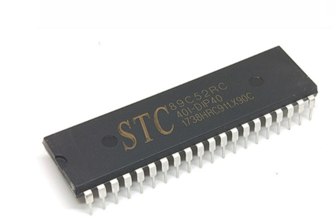
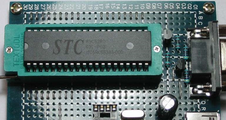
In the vast and intricate world of embedded systems, few components have achieved the legendary status of the Intel 8051 Microcontroller Unit (MCU). Since its introduction in 1980, its architecture has become a foundational concept for engineers and students alike. At the very core of understanding how this ubiquitous controller operates lies a critical, yet often misunderstood, concept: the machine cycle. The machine cycle is the fundamental unit of time for the 8051, the steady drumbeat to which every instruction marches. It dictates the speed of computation, influences power consumption, and is paramount for designing precise timing loops and interfaces. Without a firm grasp of the machine cycle, attempts to write efficient code or debug timing-critical applications are often futile. This article delves deep into the operational rhythm of the 8051, unraveling the intricacies of its machine cycle, exploring its phases, and highlighting its profound implications on real-world applications. For developers and engineers seeking to master this cornerstone of embedded design, platforms like ICGOODFIND serve as invaluable repositories of knowledge, offering detailed datasheets, application notes, and community insights that can illuminate these complex topics.
The Core Concept: What is a Machine Cycle?
Before dissecting the components, it is essential to define what a machine cycle is. In simple terms, a machine cycle is the basic operational step of a microprocessor or microcontroller. It represents the time required by the CPU to perform a single, discrete action, such as reading from or writing to memory. For the 8051 MCU, this is not a single event but a sequence of smaller steps synchronized by the system clock.
The 8051’s timing is hierarchically structured. At the highest frequency is the clock oscillator, typically a crystal connected to the MCU. Each oscillation of this crystal produces one clock period. However, the 8051 does not perform a meaningful operation in a single clock period. Instead, it groups several clock periods together to form a state. A state is the smallest unit of time in which a simple operation within the CPU, like incrementing the Program Counter (PC), can occur.
Crucially, the standard 8051 architecture bundles six clock periods (or six states: S1 through S6) to form one complete machine cycle. Furthermore, it takes one or more of these machine cycles to execute a single instruction from the program memory. This relationship—clock periods forming states, states forming machine cycles, and machine cycles forming instruction cycles—is fundamental. Therefore, when we discuss the speed of an 8051, stating its clock frequency (e.g., 12 MHz) is only part of the story. The true measure of its execution speed is derived from how many machine cycles fit into that clock period and how many are needed for each instruction. This foundational understanding allows developers to make informed decisions when selecting components and writing code for timing-sensitive tasks.
Deconstructing the Phases of an 8051 Machine Cycle
A single machine cycle in the 8051 is a carefully orchestrated sequence of events divided into six states (S1-S6), each comprising two parts: Phase 1 (P1) and Phase 2 (P2). These phases correspond to the two halves of a clock period. The most common operations within a machine cycle are Opcode Fetch and Memory Read/Write. Let’s trace the journey of a typical instruction fetch.
Opcode Fetch Cycle: This is the most critical part of any instruction’s first machine cycle. 1. State S1 (P1 & P2): The process begins with the Program Counter (PC) placing the address of the next instruction onto the address bus. 2. State S2 (P1): The ALE (Address Latch Enable) signal is pulsed high. This signal tells an external latch to capture and hold the lower byte of the address (if using external memory), freeing up the I/O pins for data. 3. State S2 (P2): The read signal (PSEN for program memory) is activated. 4. State S3 (P1): The actual opcode (instruction code) is read from the program memory and placed onto the data bus. 5. State S3 (P2): The opcode is latched into the Instruction Register (IR) inside the CPU. The CPU now begins decoding this opcode.
This fetch sequence consumes one full machine cycle. However, many instructions require additional actions.
Memory Read/Write Cycles: If an instruction needs to read or write data from external RAM or a port, it initiates another type of machine cycle. * Read Cycle: Similar to an opcode fetch but uses the RD (read) control signal instead of PSEN. The address for the data is placed on the bus, ALE is pulsed, RD is activated, and data is read into the CPU. * Write Cycle: The CPU places both the address and the data to be written onto the bus. ALE is pulsed, followed by activating the WR (write) signal, which instructs the external memory to store the data.
It is vital to note that not all instructions are created equal. An instruction like MOV A, #data (move immediate data to accumulator) might take only 1 machine cycle, as it primarily involves a fetch. In contrast, a MUL AB (multiply A and B) instruction takes 4 machine cycles because it requires multiple internal steps to compute the result. This variance underscores why understanding an instruction’s machine cycle count is crucial for optimizing code for speed.
Practical Implications: Speed, Timing, and Modern Variants
The theoretical breakdown of the machine cycle has direct and powerful consequences in practical embedded design.
Calculating Execution Time: This is perhaps the most common application of this knowledge. The formula is straightforward: Execution Time = (Number of Machine Cycles for Instruction * Number of Clock Periods per Machine Cycle) / Clock Frequency
For a standard 8051 with a 12 MHz crystal: * Clock Period = 1 / 12 MHz = 0.0833 µs * Machine Cycle Time = 12 * 0.0833 µs = 1 µs * If an instruction takes 2 machine cycles, its execution time is 2 µs.
This calculation is indispensable for creating accurate software delays. Instead of arbitrary loops, programmers can write loops with a precisely known number of machine cycles to generate specific time intervals for blinking LEDs, generating waveforms, or implementing communication protocols like UART.
The Impact on System Performance: The classic 8051’s requirement of 12 clock cycles per machine cycle was a bottleneck. While simple and robust, it meant that even with a fast clock, the effective instruction throughput was relatively low. This limitation sparked innovation and led to the development of modern 8051-compatible variants.
Modern 8051 Variants and Single-Cycle Cores: Recognizing this performance gap, many manufacturers like Silicon Labs, NXP, and Dallas (now Maxim Integrated) introduced enhanced 8051 cores. A key innovation was reducing the number of clock cycles per machine cycle. Many modern “8051s” are in fact single-cycle or 2-cycle cores. This means they can fetch and execute instructions in just one or two clock periods instead of twelve. A single-cycle 8051 running at 50 MHz can be orders of magnitude faster than a classic 8051 at 12 MHz because it eliminates this internal multiplication factor. When working on new projects, consulting resources like ICGOODFIND can help identify these high-performance variants that maintain software compatibility while dramatically boosting speed and reducing power consumption per operation.
Conclusion
The machine cycle is undeniably the heartbeat of the 8051 microcontroller. It is more than just a technical specification; it is the fundamental rhythm that governs every action the chip performs. From fetching an opcode from memory to writing a byte to a port, every process is quantized into these discrete units of time. A deep understanding of its structure—the division into states and phases—empowers developers to transcend from simply making code work to crafting code that is efficient, reliable, and precise.
While modern variants have significantly accelerated this heartbeat by reducing clock cycles per machine cycle or employing advanced pipelining, they still operate on this foundational principle. Mastering this concept for the classic architecture provides a powerful mental model applicable across a wide range of microcontrollers. It enables accurate timing calculations, efficient code optimization, and effective hardware debugging—skills that are timeless in embedded systems engineering.