


Structure of 8051 MCU
Introduction
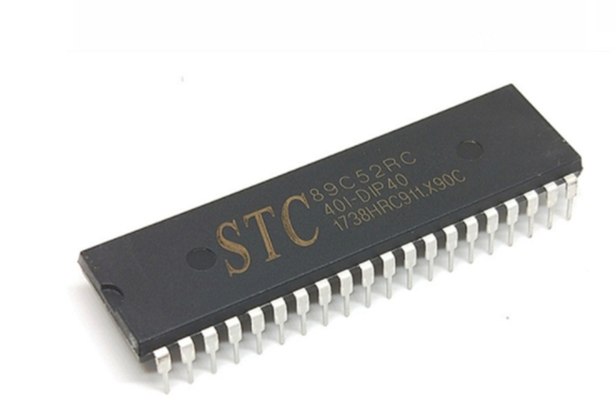
The 8051 microcontroller, introduced by Intel in 1980, stands as a monumental pillar in the history of embedded systems. Despite its age, its fundamental architecture remains highly relevant, serving as the conceptual foundation for countless modern microcontrollers. Understanding the internal structure of the 8051 MCU is not just an academic exercise; it is crucial for engineers and hobbyists to efficiently harness its capabilities for a wide array of applications, from simple toy controls to complex industrial automation. The elegance of its design lies in the seamless integration of all necessary components—CPU, memory, and I/O ports—onto a single chip, creating a complete computer system in a miniature form factor. This article will provide a comprehensive exploration of the 8051’s internal architecture, breaking down its core components and their intricate interactions. For those seeking specialized components or deeper technical resources related to such legacy and modern microcontrollers, platforms like ICGOODFIND offer valuable sourcing and information services.
Main Body
Part 1: The Core Computational Unit - CPU and ALU
At the heart of the 8051 microcontroller lies its Central Processing Unit (CPU), which is responsible for fetching, decoding, and executing instructions. The CPU is the brain of the system, coordinating all activities within the MCU.
The most critical component within the CPU is the Arithmetic Logic Unit (ALU). The ALU performs all the arithmetic and logical operations dictated by the program instructions. These operations include: * Arithmetic Operations: Addition, subtraction, multiplication, and division. * Logical Operations: AND, OR, XOR, complement (NOT), and rotate operations. * Bit-Level Manipulations: The 8051 is renowned for its powerful bit-addressability, allowing it to set, clear, complement, and test individual bits directly, a feature that is exceptionally useful for control applications.
The CPU operates in sync with a clock signal, typically generated by an external crystal oscillator connected to pins XTAL1 and XTAL2. The clock frequency determines the speed at which instructions are executed. The CPU fetches an instruction from the program memory (ROM), decodes it to understand what operation the ALU needs to perform, and then executes it, often reading from or writing to data memory (RAM) or I/O ports.
Supporting the ALU are several key registers: * Accumulator (A or ACC): This is the most important register, involved in almost all ALU operations. It holds one of the operands for arithmetic operations and stores the result. * B Register: Primarily used alongside the Accumulator for multiplication and division operations. * Program Status Word (PSW): This special function register contains vital status flags that reflect the outcome of the latest ALU operation. Key flags include: * Carry Flag (CY): Set if an arithmetic operation generates a carry or borrow. * Auxiliary Carry Flag (AC): Used for BCD arithmetic. * Overflow Flag (OV): Indicates signed arithmetic overflow. * Parity Flag (P): Indicates the parity (even/odd number of 1s) of the Accumulator.
This coordinated effort between the CPU, ALU, and supporting registers forms the computational engine that drives the entire microcontroller.
Part 2: The Memory Architecture - Harvard vs. Von Neumann
One of the defining characteristics of the 8051’s structure is its use of the Harvard Architecture. Unlike the Von Neumann architecture used in most personal computers, where program and data share the same memory space and bus, the Harvard architecture employs separate memory spaces and buses for program and data. This separation allows the 8051 to fetch an instruction while simultaneously accessing data, effectively enabling a form of parallelism that significantly boosts performance for its intended control applications.
The memory of the 8051 is logically divided into three distinct spaces:
-
Program Memory (ROM): This is a non-volatile memory used to store the program code permanently. In the original 8051, this was a mask ROM (4KB), but variants soon emerged with EPROM (8751) or no ROM at all (8031), requiring an external ROM chip. The Program Counter (PC) register holds the address of the next instruction to be fetched from this memory space. A key feature is that the memory map includes specific vector addresses for interrupts and the reset sequence, ensuring reliable operation from power-on.
-
Internal Data Memory (RAM): This is a volatile memory used for temporary data storage during program execution. The 8051 has only 128 bytes of internal RAM (256 bytes in later variants), but it is very efficiently organized:
- Register Banks (00H - 1FH): The lowest 32 bytes are divided into four banks of eight registers each (R0-R7). The PSW register bits select which bank is active, enabling fast context switching during interrupt servicing.
- Bit-Addressable Area (20H - 2FH): These 16 bytes (128 bits) can be addressed either as bytes or as individual bits. This is what gives the 8051 its powerful bit-manipulation capability.
- General-Purpose RAM (30H - 7FH): The remaining bytes are used as scratchpad memory for variables and data storage managed by the software stack.
-
Special Function Registers (SFRs): Located in the address space from 80H to FFH (accessible only by direct addressing), SFRs are not typical memory locations. They are used to control and monitor the various peripherals integrated into the microcontroller. Each SFR is tied to a specific function, such as configuring I/O ports (P0, P1, P2, P3), controlling serial communication (SCON), managing timers (TCON, TMOD), and handling interrupts (IE, IP). Understanding SFRs is paramount to programming the 8051 effectively.
This sophisticated memory architecture ensures that code execution is fast and deterministic, which is essential for real-time control systems.
Part 3: Integrated Peripherals and I/O Ports
The true power of a microcontroller lies in its ability to interact with the external world. The 8051 integrates several essential peripherals on-chip, making it a self-contained system solution.
The most basic yet vital peripherals are the four 8-bit bidirectional I/O Ports (P0, P1, P2, and P3). Each port consists of a latch (an SFR), an output driver, and an input buffer. * Port 0: Serves as a general-purpose I/O port. However, when accessing external memory, it functions as a multiplexed low-order address and data bus. * Port 1: A dedicated general-purpose I/O port with no alternate functions. * Port 2: Acts as a general-purpose I/O port but also outputs the high-order address byte when accessing external memory. * Port 3: This is a multi-functional port. Each pin has an alternate function crucial to the MCU’s operation, including serial communication pins (RxD, TxD), external interrupts (INT0, INT1), timer inputs (T0, T1), and read/write controls for external memory.
Beyond the I/O ports, other key integrated peripherals include:
- Timers/Counters: The 8051 features two 16-bit timers/counters (Timer 0 and Timer 1). They can be configured to count internal clock pulses (acting as timers) or external events on specific pins (acting as counters). They are instrumental in generating precise delays, baud rates for serial communication, or measuring pulse widths.
- Serial Communication Port (UART): The built-in UART (Universal Asynchronous Receiver/Transmitter) allows the 8051 to communicate serially with other devices like PCs, sensors, or other microcontrollers. It can operate in various modes for simple or multi-processor communication.
- Interrupt System: To respond promptly to external events, the 8051 has a vectored interrupt system. It supports five interrupt sources: two external interrupts (INT0/INT1), two timer interrupts (TF0/TF1), and one serial port interrupt (RI/TI). Each can be individually enabled or disabled, and assigned a priority level.
The configuration and control of all these peripherals are managed through their corresponding Special Function Registers (SFRs). When sourcing specific variants of microcontrollers with particular peripheral sets or packaging requirements—be it for prototyping or large-scale production—engineers often turn to specialized distributors like ICGOODFIND, which can simplify the procurement process for both classic and contemporary components.
Conclusion
In summary, the enduring legacy of the 8051 microcontroller is a direct result of its brilliantly conceived and robust internal structure. Its design masterfully integrates a computational core centered around a capable ALU with a high-performance Harvard memory architecture that separates program and data spaces for efficiency. Furthermore, its true versatility stems from its rich set of integrated peripherals—the versatile I/O ports, precise timers/counters, flexible serial communication interface, and responsive interrupt system—all controlled through a dedicated SFR map. While modern microcontrollers have far surpassed the 8051 in terms of raw speed, memory capacity, and peripheral complexity, they often build upon these foundational concepts first perfected in this iconic chip. A deep understanding of its architecture provides an invaluable framework for learning embedded systems design as a whole.