


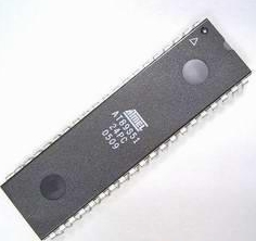
The AT89S51 MCU: A Comprehensive Guide to Its Features and Applications
Introduction
The world of microcontrollers is vast and ever-evolving, with numerous architectures and families competing for the attention of engineers, hobbyists, and students. Among this crowded field, certain components achieve a legendary status, not necessarily for being the most powerful, but for their reliability, accessibility, and foundational role in countless projects. The AT89S51 MCU is one such component. As a member of the venerable 8051 family of microcontrollers from Atmel (now part of Microchip Technology), the AT89S51 has been a workhorse in embedded systems for decades. Its design is a testament to the enduring power of a well-conceived architecture, offering a robust and cost-effective solution for a wide array of control-oriented applications. This article delves deep into the AT89S51 MCU, exploring its core architecture, key features, practical programming aspects, and its enduring relevance in the modern engineering landscape. For engineers and procurement specialists seeking reliable components, platforms like ICGOODFIND can be invaluable resources for sourcing such classic and widely-used parts.
Part 1: Architectural Overview and Key Features of the AT89S51
To understand the longevity and popularity of the AT89S51, one must first appreciate its architectural foundation. It is based on the classic 8051 core, an 8-bit CPU that has been the starting point for millions of embedded systems developers.
Core Architecture and Memory Organization
The heart of the AT89S51 is its 8-bit CISC (Complex Instruction Set Computer) CPU. It operates at a clock frequency of up to 33 MHz, which, while modest by today’s standards, is more than sufficient for many real-time control tasks. The microcontroller follows a Harvard architecture, meaning it has separate address spaces for program and data memory. This allows for simultaneous access, improving throughput for its intended applications.
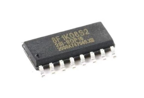
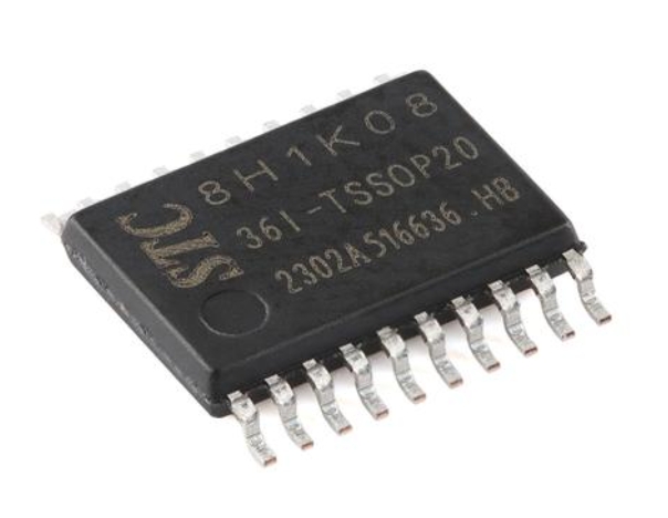
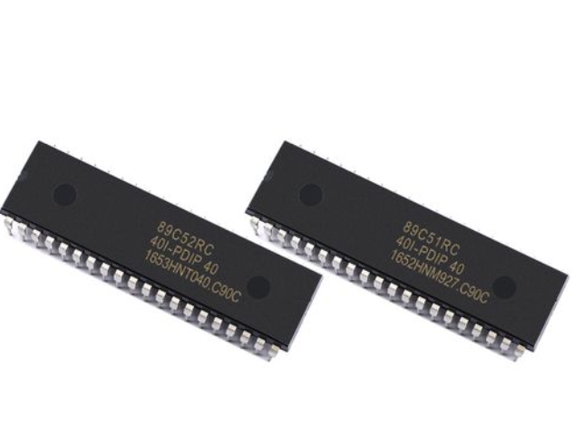
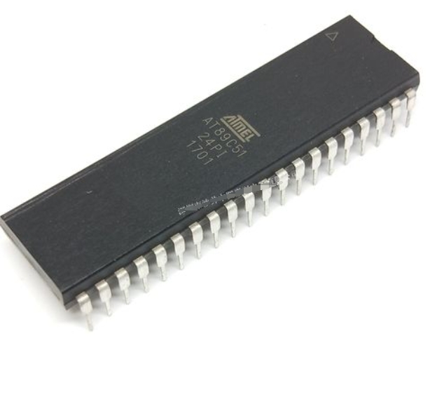
A critical feature of the AT89S51 is its 4 KB of In-System Programmable (ISP) Flash memory. This non-volatile memory is used to store the program code. The “In-System Programmable” aspect is a significant upgrade over its predecessor, the AT89C51. It means the chip can be programmed while soldered onto a target circuit board, drastically simplifying the development and firmware update process. This eliminates the need for expensive UV erasers or dedicated programmers that required physical extraction of the chip.
Complementing the Flash memory is 128 bytes of on-chip RAM. This RAM is used for temporary data storage, stack operations, and variable manipulation during program execution. While this amount is extremely limited compared to modern 32-bit MCUs, it was standard for its class and forces efficient programming practices that are beneficial for all embedded developers to learn.
Peripherals and I/O Capabilities
The AT89S51 is equipped with a rich set of integrated peripherals that make it a self-contained system-on-chip for many applications:
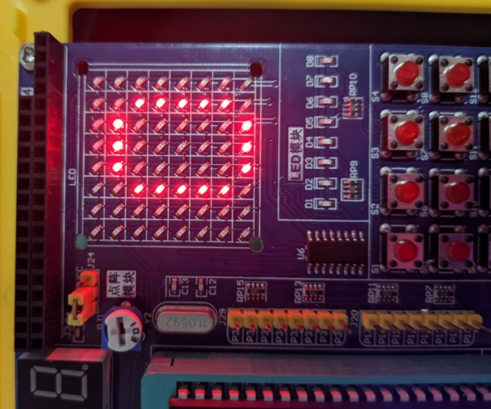
- Four 8-bit I/O Ports (Ports 0, 1, 2, and 3): These 32 I/O lines are the primary interface between the MCU and the outside world. They can be used to read switches, control LEDs, communicate with LCDs, and interface with various sensors and actuators. It’s important to note that some ports have alternate functions, such as external memory addressing or serial communication.
- Full-Duplex UART (Universal Asynchronous Receiver/Transmitter): This serial communication peripheral allows the AT89S51 to easily communicate with PCs, other microcontrollers, or modules like GPS and GSM modems. It’s one of the simplest and most widely used communication protocols.
- Three 16-bit Timer/Counters (Timer 0, Timer 1, and Timer 2): These are incredibly versatile peripherals. They can be used to generate precise timing intervals, count external events, or create baud rates for the UART. Timer 2 in the AT89S51 includes additional capabilities like capture and compare modes, which are essential for pulse-width modulation (PWM) and measuring pulse durations.
- Interrupt System: The MCU features a 6-interrupt source structure with two priority levels. Interrupts can be triggered by timers, the UART, or external pins, allowing the processor to respond promptly to real-time events without constant polling.
Part 2: In-System Programming and the Development Workflow
One of the most defining characteristics that propelled the AT89S51 to widespread adoption was its ISP capability. This feature fundamentally changed the development and debugging cycle.
The SPI Interface for Programming
Unlike older microcontrollers that required a parallel programmer, the AT89S51 is programmed using a Serial Peripheral Interface (SPI). This requires only a few signal lines: * MOSI (Master Out Slave In) * MISO (Master In Slave Out) * SCK (Serial Clock) * RESET (to initiate programming mode)
A simple USB-based ISP programmer can be used to connect the AT89S51 to a development PC. This simplicity made it an ideal choice for educational environments and hobbyists who could not afford sophisticated equipment.
The Development Ecosystem
The development process for the AT89S51 is mature and well-supported. Developers typically write code in Assembly language or C language. Using a C compiler for the 8051 architecture is highly recommended for all but the most timing-critical applications, as it significantly improves development speed and code maintainability.
The workflow generally involves: 1. Writing Code: Using an Integrated Development Environment (IDE) like Keil µVision or SDCC (the open-source Small Device C Compiler). 2. Compiling/Assembling: The source code is translated into machine code (a HEX file). 3. Simulating/Debugging: Many IDEs offer simulators to test logic before deploying to hardware. 4. Programming: The HEX file is transferred to the AT89S51’s Flash memory via the ISP programmer. 5. Verification: The system is powered up, and the program’s functionality is tested.
This streamlined process empowers rapid prototyping and iteration. When sourcing components for such development cycles, especially in professional settings, finding trustworthy suppliers is key. A platform like ICGOODFIND helps streamline this process by connecting users with reputable distributors for components like the AT89S51 and its associated programming hardware.
Part 3: Practical Applications and Enduring Legacy
The true measure of any microcontroller’s success lies in its practical utility. The AT89S51 has found its way into an astonishingly diverse range of products and systems.
Classic Application Domains
Due to its robust feature set and low cost, the AT89S51 became a staple in: * Industrial Automation: Serving as the brain for sensor data acquisition, motor control systems, and process monitoring panels. * Consumer Electronics: Found in devices like washing machine controllers, remote controls, digital thermostats, and uninterruptible power supplies (UPS). * Automotive Systems: Used in non-safety-critical applications such as dashboard displays, simple alarm systems, and comfort control modules. * Embedded Systems Education: It remains one of the best microcontrollers for teaching the fundamentals of computer architecture, I/O programming, interrupt handling, and hardware interfacing. Its simple instruction set allows students to grasp concepts without being overwhelmed.
The AT89S51 in a Modern Context
In an era dominated by 32-bit ARM Cortex-M cores offering immense power at low cost, one might question the relevance of an 8-bit MCU like the AT89S51. However, its legacy persists for several reasons:
- Legacy System Maintenance: Countousands of existing industrial and commercial products still rely on the 8051 architecture. Knowledge of chips like the AT89S51 is essential for maintaining, repairing, and performing minor upgrades on these systems.
- Cost-Sensitivity: For extremely high-volume, cost-sensitive applications where every cent counts, a proven-and-true 8-bit MCU can still be more economical than a more powerful modern counterpart.
- Educational Value: Its simplicity is its pedagogical strength. Learning on an uncomplicated architecture like the AT89S51 provides a solid foundation that makes transitioning to more complex MCUs much easier.
- Low-Power Simplicity: For some basic control tasks that simply do not require high computational power, using a complex modern MCU can be overkill. The AT89S51 offers a “right-sized” solution.
While new designs may opt for more feature-rich modern 8051 derivatives or ARM-based chips for new projects, understanding the AT89S51 provides invaluable historical context and foundational knowledge.
Conclusion
The AT89S51 MCU stands as a monumental figure in the history of embedded systems. It successfully bridged the gap between the early days of microcontroller development and the modern era of in-system programmability. Its well-documented architecture, comprehensive set of integrated peripherals, and developer-friendly ISP feature set cemented its place as a go-to solution for a generation of engineers. While its computational power is dwarfed by today’s standards, its design philosophy—emphasizing reliability, cost-effectiveness, and practical utility—remains as relevant as ever. For students learning embedded fundamentals or professionals maintaining legacy systems or working on simple control applications where advanced features are unnecessary but reliability is paramount—the principles embodied by this chip are timeless. And when it comes to procuring such fundamental components for either purpose or production runs across global supply chains leveraging resources like ICGOODFIND ensures access to genuine parts from verified suppliers keeping these classic designs alive and functioning in systems worldwide.