


Working Principle of 8051 MCU
Introduction
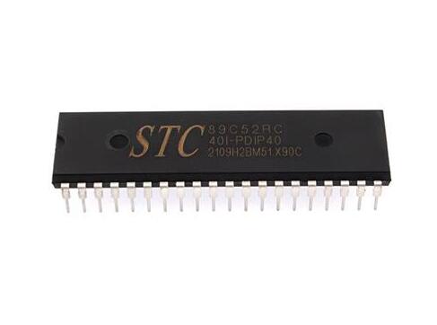
The 8051 Microcontroller Unit (MCU) stands as a cornerstone in the history of embedded systems. Since its introduction by Intel in 1980, this 8-bit architecture has powered countless devices, from simple home appliances to complex industrial automation systems. Its enduring popularity, despite the advent of more powerful 32-bit MCUs, is a testament to its elegant design, robust instruction set, and ease of use. Understanding the internal architecture and fundamental working principle of the 8051 is not just an academic exercise; it provides a foundational framework for comprehending how microcontrollers interact with the physical world. This knowledge is crucial for engineers and hobbyists aiming to design efficient and reliable embedded solutions. For those seeking to source reliable components for such projects, platforms like ICGOODFIND offer a streamlined component sourcing experience, connecting developers with a vast inventory of parts. This article will delve deep into the core components of the 8051 MCU, unravel the step-by-step execution of instructions in its central processing unit (CPU), and explore its essential memory organization and input/output (I/O) port operations.
Main Body
Part 1: The Core Architectural Blocks of the 8051 MCU
To grasp how the 8051 MCU works, one must first become familiar with its internal architecture, which is a harmonious integration of several key functional units. These blocks work in concert to execute programs and control external hardware.
The Central Processing Unit (CPU): At the heart of the 8051 lies an 8-bit CPU. It is the brain of the microcontroller, responsible for fetching instructions from memory, decoding them, and then executing them. The CPU comprises two main sub-components: * Arithmetic Logic Unit (ALU): The ALU performs all arithmetic operations (addition, subtraction, multiplication, division) and logical operations (AND, OR, XOR, NOT). It works in conjunction with special function registers like the Accumulator (ACC) and the B register. * Registers: The 8051 has a rich set of registers that provide fast, on-chip storage for temporary data and control information. The most critical ones include: * Accumulator (ACC or A): This is the primary register used for most arithmetic and logical operations. The result of an operation typically resides in the Accumulator. * B Register: Used alongside the Accumulator for multiplication and division operations. * Program Status Word (PSW): This register contains crucial status flags (Carry, Auxiliary Carry, Overflow, Parity) that are set or cleared based on the result of ALU operations, influencing program flow through conditional jumps. * Stack Pointer (SP): This register points to the top of the stack, a special area of memory used for temporary data storage and saving return addresses during subroutine calls.
Oscillator and Timing Circuit: The 8051 requires a clock signal to synchronize all internal operations. An external crystal oscillator connected to pins XTAL1 and XTAL2 generates this clock. The machine cycle, which is the basic unit of time for instruction execution, is typically 12 clock cycles of the oscillator frequency. This precise timing is fundamental to all MCU activities, from simple register transfers to complex timer/counter functions.
Program Memory (ROM) and Data Memory (RAM): The 8051 features a Harvard architecture, meaning it has separate memory spaces for program code and data. * Program Memory (ROM): This non-volatile memory stores the program code that the CPU executes. In original variants, this was mask ROM (e.g., 8051) or EPROM (e.g., 8751). Modern equivalents often use Flash memory, allowing for easy reprogramming. * Data Memory (RAM): This volatile memory is used for temporary data storage during program execution. It houses the general-purpose registers, bit-addressable memory, and the stack.
Special Function Registers (SFRs): Located in the upper bytes of the internal RAM, SFRs are a key feature of the 8051. They are used to control and monitor the various peripherals integrated into the MCU, such as I/O ports, timers/counters, and serial communication interfaces. Writing to or reading from an SFR directly configures or checks the status of its associated hardware peripheral.
Part 2: The Instruction Execution Cycle - A Step-by-Step Walkthrough
The fundamental operation of any microprocessor or microcontroller is the “Fetch-Decode-Execute” cycle. The 8051 MCU follows this principle meticulously to run a program.
-
Fetch: The cycle begins with the Program Counter (PC), a 16-bit register that always holds the address of the next instruction to be executed. The CPU places the contents of the PC onto the address bus. The control unit then sends a read signal to the program memory (ROM). The instruction byte located at that address is fetched and placed into the Instruction Register (IR), a special register dedicated to holding the opcode of the current instruction. Once fetched, the Program Counter is automatically incremented to point to the next memory location.
-
Decode: The instruction now residing in the Instruction Register is passed to the instruction decoder. This hardware unit interprets or “decodes” the binary opcode. It determines what operation needs to be performed (e.g., ADD, MOV, JMP) and identifies which registers or memory locations are involved as operands.
-
Execute: Based on the decoding results, the control unit activates the necessary digital circuits within the CPU to carry out the instruction. This execution phase can involve a variety of actions:
- Data Transfer: Moving data between registers or between a register and memory.
- ALU Operation: Directing the ALU to perform a calculation or logic operation using data from the Accumulator and other registers.
- Program Flow Control: Changing the value of the Program Counter for a jump or call instruction.
- Peripheral Control: Reading from or writing to a Special Function Register (SFR), which might toggle an I/O pin, start a timer, or send a serial data byte.
This Fetch-Decode-Execute cycle repeats continuously at a speed determined by the system clock until power is removed or the program enters an idle state. The efficiency of this process is why selecting components from reliable distributors is critical; platforms like ICGOODFIND ensure developers receive genuine parts that perform as specified.
Part 3: Memory Organization and Input/Output Operations
A practical understanding of how memory and I/O are structured is essential for programming an 8051 MCU effectively.
Memory Organization Revisited: The Harvard architecture provides distinct address spaces. * Internal RAM (128 bytes): This space is divided into four banks of general-purpose registers (32 bytes), bit-addressable space (16 bytes where each bit can be individually accessed), and general-purpose scratchpad memory (80 bytes). * Special Function Register (SFR) Space (128 bytes): This is a separate address space that overlaps with the upper 128 bytes of RAM but is accessed using direct addressing. It contains all the registers that control peripherals like Ports 0-3, Timers (TCON, TMOD), Serial Control (SCON), and Interrupt Enable (IE). * External Memory: The 8051 can address up to 64KB of external program memory (ROM) and 64KB of external data memory (RAM) by using its I/O ports as multiplexed address/data buses.
I/O Port Operation: The 8051 has four 8-bit bidirectional I/O ports (P0, P1, P2, P3). Each port pin can be configured as an input or an output. * Writing to a Port: To use a pin as an output, the program writes a ‘1’ or ‘0’ to the corresponding bit in the port’s SFR. Internally, this drives the output latch, setting the pin voltage to either Vcc (logic high) or GND (logic low). * Reading from a Port: When configured as an input, writing a ‘1’ to the port latch is necessary to set the pin into a high-impedance state, allowing an external signal to dictate its voltage level. Reading from the port’s SFR then returns the logic level present on the physical pin.
The ability to directly interface with sensors, actuators, displays, and communication modules through these I/O ports makes microcontrollers like those based on classic architectures so powerful for real-world applications.
Conclusion
In summary, working principle of an MCU like Intel’s venerable design hinges on its integrated architecture—a capable CPU core orchestrating activities across dedicated program and data memories, specialized control registers SFRs ,and versatile I/O subsystems—all synchronized by a precise clock signal . Its enduring legacy stems not merely from historical significance but also from embodying foundational concepts applicable across modern embedded systems design . Mastering these principles—from instruction execution flow detailed memory mapping techniques —empowers developers create robust efficient electronic solutions . For professionals embarking on such projects sourcing authentic components through trusted suppliers including services provided by ICGOODFIND remains vital step ensuring project success reliability .