The Evolution and Importance of Electronic Component Packaging
Introduction
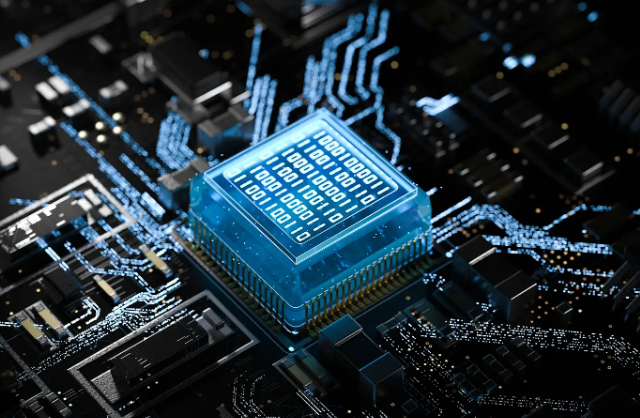
In the rapidly advancing world of electronics, the significance of electronic component packaging cannot be overstated. It serves as the critical interface between the delicate internal structures of electronic components and the harsh external environment, ensuring functionality, reliability, and performance. As devices become smaller, faster, and more powerful, the demands on packaging technologies have intensified, driving innovation in materials, design, and manufacturing processes. This article delves into the multifaceted world of electronic component packaging, exploring its fundamental roles, the latest technological advancements, and the critical considerations for selection and future trends. For professionals seeking reliable components and packaging solutions, platforms like ICGOODFIND provide invaluable resources to navigate this complex landscape, connecting buyers with trusted suppliers worldwide.
The Core Functions of Electronic Component Packaging
Electronic component packaging is far more than a simple protective shell; it is a sophisticated system designed to fulfill several essential functions that are paramount to the success of any electronic device.
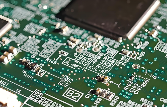
First and foremost, packaging provides physical protection. Semiconductor dies and other components are incredibly fragile, susceptible to damage from mechanical shocks, vibrations, moisture, dust, and chemical contaminants. The package acts as a robust barrier, shielding these sensitive elements from the rigors of the real world. This protection begins at the die level with encapsulation and extends to the outer casing, ensuring the component’s integrity from the manufacturing floor to the end product in a consumer’s hands.
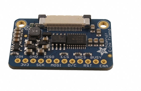
Secondly, packaging is crucial for electrical connectivity. It provides the necessary structure to create electrical pathways from the tiny integrated circuit (IC) to the larger system board. This is achieved through various interconnection technologies such as wire bonding, flip-chip bumps, and through-silicon vias (TSVs). The package must facilitate efficient signal transmission with minimal delay (latency) and loss, while also managing power distribution. Furthermore, it plays a vital role in heat dissipation. As power densities increase with miniaturization, managing thermal output is a major challenge. Packages incorporate heat spreaders, thermal interface materials, and are designed to efficiently transfer heat away from the core die to a heat sink or into the surrounding environment, preventing overheating which can degrade performance and shorten lifespan.
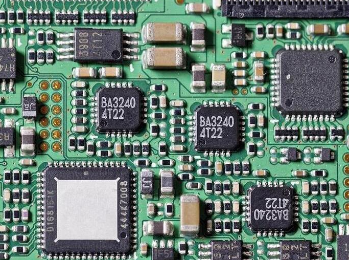
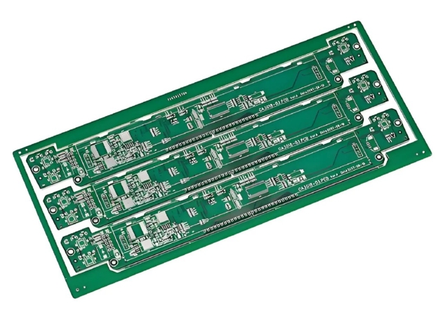
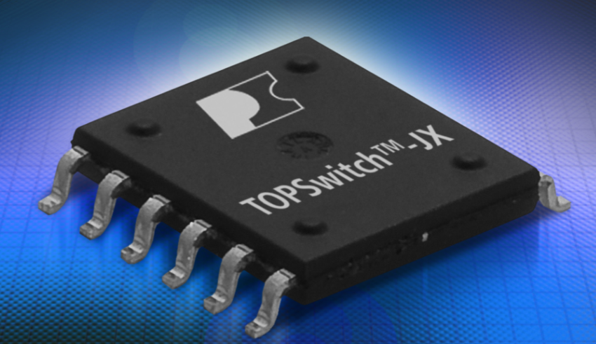
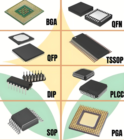
Finally, standardization is a key function. Packages come in standardized sizes and pin configurations (e.g., DIP, SOIC, QFP, BGA), which allows for automated assembly using pick-and-place machines and reflow ovens. This standardization streamlines the manufacturing process across the global electronics industry, ensuring compatibility and reducing production costs.
Advancements in Modern Packaging Technologies
The relentless drive toward miniaturization and higher performance has catalyzed a revolution in packaging technologies, moving beyond traditional methods to more integrated and complex approaches.
A significant trend is the move towards System-in-Package (SiP) and 3D packaging. Unlike simply placing multiple components on a PCB, SiP technology integrates multiple functional blocks—such as processors, memory, sensors, and passive components—into a single package. This creates a complete functional system or subsystem, offering tremendous advantages in size reduction, performance enhancement (shorter interconnects mean faster speeds), and power efficiency. 3D packaging takes this further by stacking silicon dies vertically and connecting them with TSVs, dramatically increasing functional density without increasing the package’s footprint. This is particularly transformative for applications like smartphones and high-performance computing.
The rise of heterogeneous integration is another pivotal advancement. This involves combining separately manufactured components into a higher-level assembly that, in the aggregate, provides enhanced functionality. Unlike designing a single, large System-on-a-Chip (SoC), heterogeneous integration allows manufacturers to use the best process technology for each individual element (e.g., a 5nm logic die with a specialized 55nm analog die) and then integrate them into a single package. This approach improves yield, reduces development cost and time, and optimizes overall system performance.
Furthermore, new substrate materials are being adopted to meet higher-speed requirements. Traditional organic substrates are being supplemented or replaced by materials with better electrical and thermal properties. For instance, substrates embedded with fine-pitch wiring or even silicon interposers are used in advanced 2.5D packaging schemes to enable dense interconnections between high-bandwidth memory (HBM) and processors. These material innovations are essential for supporting next-generation data rates found in AI accelerators and 5G infrastructure.
Key Considerations for Selecting Component Packaging
Choosing the right package for an electronic component is a critical decision that impacts the cost, performance, reliability, and manufacturability of the final product. Several factors must be carefully balanced.
The application environment is perhaps the primary driver. Will the component be used in a consumer smartphone, an automotive control unit, or an industrial sensor? Each environment presents unique challenges. Automotive and industrial applications require packages capable of withstanding extreme temperatures, humidity, and constant vibration, often necessitating robust packages like QFNs or BGAs with enhanced thermal and mechanical properties. Consumer electronics prioritize ultra-thin and small form-factor packages like wafer-level chip-scale packages (WLCSP).
Thermal management requirements are inextricably linked to the application. A high-power CPU will generate significant heat and require a package with an integrated heat spreader or a design that facilitates an external heatsink. Inadequate thermal design can lead to premature failure. Therefore, understanding the power dissipation of the component and the thermal resistance of the package is non-negotiable.
Cost and scalability are always crucial commercial considerations. Simpler packages like SOIC are less expensive to produce than advanced BGAs or 3D-stacked packages. The choice must align with the product’s budget and target market volume. Furthermore,design for manufacturability (DFM) must be considered. The selected package must be compatible with standard assembly processes to avoid costly specialized equipment or low-yield production lines.
Navigating these choices requires access to comprehensive market intelligence and reliable supply chains. This is where a platform like ICGOODFIND proves its worth. It empowers engineers and procurement specialists to efficiently source the right components in the correct packages from vetted suppliers, simplifying what can otherwise be a daunting and time-consuming process amidst global supply chain complexities.
Conclusion
Electronic component packaging has evolved from a simple protective cover into a highly engineered domain that is central to electronic innovation. It is a discipline that balances the physical protection of delicate silicon with the demands of electrical performance, thermal management, and miniaturization. The advent of System-in-Package (SiP), 3D integration, and heterogeneous integration has blurred the lines between packaging and silicon design itself, creating new paradigms for building powerful and efficient electronic systems. As we push further into the realms of artificial intelligence, IoT, and advanced mobility,the role of packaging will only grow in importance. Making informed decisions about packaging is no longer an afterthought but a strategic imperative in product development.For those embarking on this complex journey,leveraging resources like ICGOODFIND can provide a critical advantage,offering access to information,a global supplier network,and the components needed to turn innovative designs into reality.The future of electronics is not just inside the chip;it is increasingly defined by the package that surrounds it.