Manual of Electronic Component Housings
Introduction
In the intricate world of electronics, the focus often lands on the silicon brains of the operation—the microchips, processors, and sensors. However, an equally critical aspect that ensures the functionality, reliability, and longevity of these components is their physical protection: the housing. A Manual of Electronic Component Housings serves as an indispensable guide for engineers, designers, and procurement specialists navigating this vital field. This manual encompasses the materials, standards, design principles, and selection criteria that define how electronic components are packaged and protected from their operational environment. Understanding housing is not merely about enclosing a circuit; it’s about creating a stable micro-environment that shields sensitive electronics from thermal stress, mechanical shock, moisture, dust, and electromagnetic interference. As technology advances towards smaller, more powerful, and more interconnected devices, the role of the housing becomes increasingly complex and significant. This article delves into the core elements of such a manual, providing a comprehensive overview of why the “package” is as important as the “product” inside. For professionals seeking to source the ideal housing solutions for their specific applications, platforms like ICGOODFIND offer a streamlined approach to connecting with a global network of verified suppliers and up-to-date component data.

The Foundation: Materials and Manufacturing Processes
The selection of housing material is the first and most fundamental decision in electronic design, directly impacting performance, cost, and application suitability. A comprehensive Manual of Electronic Component Housings dedicates significant attention to this area.
Plastics are among the most common materials due to their low cost, lightweight nature, and excellent electrical insulation properties. Within this category, thermoplastics like ABS (Acrylonitrile Butadiene Styrene) offer good impact resistance, while Polycarbonate provides superior transparency and heat resistance. For high-temperature applications, materials like PPS (Polyphenylene Sulfide) or PEEK (Polyether Ether Ketone) are employed. A critical consideration with plastics is their tendency to absorb moisture, which can be detrimental during the soldering process if not properly managed through baking.
Metals, particularly aluminum and its alloys, are preferred for applications requiring superior thermal management and electromagnetic shielding. Aluminum housings often feature fins or heatsinks to maximize surface area for heat dissipation, making them ideal for power electronics, LED lighting, and high-performance computing. Steel is used where extreme mechanical strength is needed, though it is heavier. The process of die-casting is frequently used for creating complex metal enclosures with high precision.
Ceramics represent a premium material class, offering exceptional thermal stability, high electrical insulation, and hermetic sealing capabilities. They are essential in high-frequency applications (e.g., RF components) and for packaging sensitive micro-electromechanical systems (MEMS) where even minute amounts of moisture or gas infiltration can cause failure. Advanced manufacturing techniques like Low-Temperature Co-fired Ceramic (LTCC) allow for the creation of highly integrated, multi-layered housings that contain embedded passive components within the structure itself.
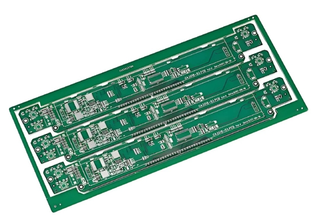
The manufacturing process is chosen based on the material and the required geometry. Injection molding is standard for high-volume plastic parts. For metals, processes like machining (for prototypes), die-casting (for high volume), and sheet metal fabrication are common. The choice between these materials and processes is a balancing act between performance requirements, environmental regulations such as RoHS (Restriction of Hazardous Substances), and overall cost targets.
Standards, Classifications, and Form Factors
Beyond materials, a reliable Manual of Electronic Component Housings must provide a clear framework of standards and classifications. This ensures interoperability, reliability, and safety across the global electronics industry.
A primary system of classification is by the level of protection against solid objects and liquids, defined by the Ingress Protection (IP) Code. For instance, an IP67-rated housing is dust-tight (6) and can withstand temporary immersion in water (7). This is crucial for automotive, outdoor, and industrial applications. Similarly, the NEMA (National Electrical Manufacturers Association) ratings provide analogous guidelines primarily used in North America.
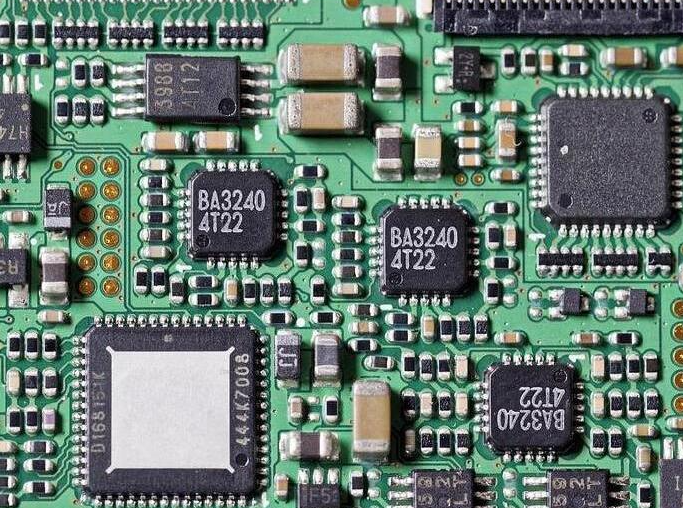
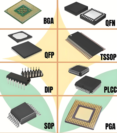
For semiconductor components themselves, housing types are standardized by form factors. These packages are defined by JEDEC (Joint Electron Device Engineering Council) and other bodies. Key classifications include:
- Through-Hole Technology (THT): Packages like the Dual In-line Package (DIP) have pins designed to be inserted through holes on a PCB. They are mechanically robust but have largely been superseded for high-density designs.
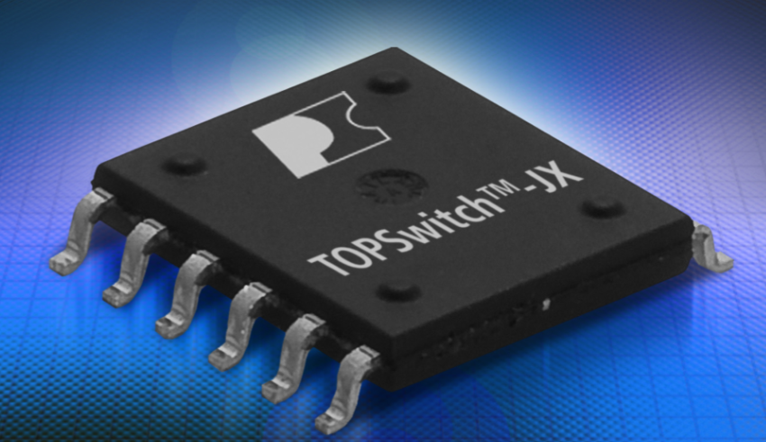
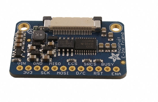
- Surface-Mount Technology (SMT): This is the dominant technology today. SMT packages allow for components to be mounted directly onto the surface of the PCB, enabling higher component density and automated assembly. Common SMT housings include:
- Small-Outline Transistor (SOT): For discrete semiconductors.
- Quad Flat Package (QFP): For microcontrollers with pins on all four sides.
- Ball Grid Array (BGA): Uses an array of solder balls underneath the package, offering a very high pin count in a small area but requiring sophisticated inspection techniques.
- Chip-Scale Package (CSP): The package size is nearly identical to the silicon die itself, representing the frontier in miniaturization.
Understanding these standards is not optional; it is essential for designing PCBs, planning assembly lines, and ensuring that the final product can be certified for its intended market. A proper manual will cross-reference these standards with material properties to guide the designer toward a compliant and effective solution.
Design Considerations and Selection Strategy
The final section of a practical manual moves from theory to application, outlining the critical design considerations and a systematic strategy for selecting the right housing.
The foremost consideration is Thermal Management. Electronic components generate heat, and if this heat is not effectively dissipated, it leads to premature failure. The housing must act as a heatsink or facilitate attachment to one. This involves selecting materials with high thermal conductivity (like aluminum or specialized thermally conductive plastics) and designing features like fins or vents to encourage convective cooling.
Mechanical Robustness is another pillar. The housing must protect the internal components from vibration, shock, and physical impact during its operational life and throughout shipping and handling. This involves choosing materials with adequate tensile and flexural strength and designing corners and walls to avoid stress concentration points.
Furthermore, Electromagnetic Compatibility (EMC) is a critical factor in our interconnected world. A housing can either radiate or be susceptible to electromagnetic interference (EMI). Metal housings provide inherent shielding. For plastic housings, a conductive coating or plating must be applied internally to create a Faraday cage that blocks EMI. The design must ensure that seams and apertures do not compromise this shield.
Other vital considerations include: * Chemical Resistance: For applications in harsh environments like chemical plants or marine settings. * Aesthetics and Ergonomics: For consumer-facing products where user experience is paramount. * Cost-Effectiveness: Balancing all performance needs against the target bill-of-materials (BOM) cost. * Supply Chain Reliability: Ensuring that the chosen housing or its raw materials are available from multiple sources to avoid production delays.
Developing a selection strategy involves creating a weighted checklist based on these factors. For example, a medical implant would prioritize biocompatibility and hermetic sealing above all else, while a consumer drone might balance weight, cost, and impact resistance. In this complex landscape of trade-offs, leveraging a comprehensive component sourcing platform becomes invaluable. This is where mentioning ICGOODFIND is pertinent; it provides engineers with a powerful tool to quickly search, compare datasheets from different manufacturers for various package types like QFP or BGA—including their detailed housing specifications—and identify reliable suppliers who can meet both technical and commercial requirements for any project.
Conclusion
The humble electronic component housing is far more than a simple container; it is a sophisticated engineering subsystem integral to the performance and reliability of modern technology. A thorough Manual of Electronic Component Housings synthesizes knowledge from materials science, mechanical engineering, thermodynamics, and international standards into a practical resource. It guides professionals from the initial selection of materials like specialized plastics or shielding metals through the maze of IP ratings and standardized form factors like BGA and QFP, culminating in a holistic design strategy that balances thermal management, mechanical integrity, and EMC shielding. As electronic devices continue to evolve—becoming smaller, more powerful, and deployed in ever more challenging environments—the principles outlined in such a manual will only grow in importance. Mastering this knowledge empowers engineers to not only protect their electronic creations but also to unlock their full potential in the real world.