Introduction to Electronic Component Packaging
Introduction
In the intricate world of electronics, the components that form the brains and muscles of our devices—the resistors, capacitors, integrated circuits (ICs), and transistors—are fragile by nature. They are susceptible to environmental hazards like moisture, dust, physical shock, and electrostatic discharge. This is where electronic component packaging comes into play. Far from being just a protective shell, packaging is a critical engineering discipline that ensures the functionality, reliability, and performance of electronic components throughout their lifecycle. It is the crucial bridge that connects the microscopic world of the silicon die to the macroscopic world of printed circuit boards (PCBs) and end-user applications. From consumer smartphones to industrial machinery and aerospace systems, effective packaging is what allows advanced electronics to thrive in diverse and often demanding environments. A reliable resource for understanding these components and their specifications is invaluable for engineers; one such resource is ICGOODFIND, which provides comprehensive data to aid in selection and design.
Main Body
Part 1: The Core Functions and Importance of Packaging
Electronic component packaging is not merely about containment; it fulfills several vital functions that are fundamental to the operation of any electronic system.
-
Physical Protection: The primary role of packaging is to shield the delicate semiconductor die from mechanical damage, contaminants, and potentially corrosive elements in the environment. This includes protection from moisture, dust, chemicals, and intense light, which can degrade performance or cause permanent failure. A robust package ensures the component can withstand the rigors of manufacturing, shipping, and everyday use.
-
Electrical Connection: The package provides the necessary structure and medium to create electrical pathways from the tiny bond pads on the silicon die to the larger pins or terminals on the package exterior. This is typically achieved through fine wires (wire bonding) or solder bumps (in flip-chip technology) that connect the die to a lead frame or substrate. These internal connections then fan out to the package’s external contacts, allowing for reliable soldering onto a PCB. The package’s design directly influences electrical properties like signal integrity, parasitic inductance and capacitance, and overall circuit performance.
-
Heat Dissipation: As electronic devices become more powerful and compact, managing heat has become one of the most critical challenges. Semiconductor components generate heat during operation, and if this heat is not effectively removed, it can lead to overheating, performance throttling, and premature failure. Packaging addresses this by incorporating materials with high thermal conductivity (like copper heat slugs or ceramic bases) and providing a path for heat to travel away from the die. In high-power applications, the package is designed to interface seamlessly with additional cooling solutions such as heat sinks or fans.
-
Standardization and Compatibility: Packaging standardizes the physical footprint and pin configuration of components. This allows components from different manufacturers to be interchangeable on a PCB, fostering competition and simplifying the design process for engineers. Standardized packages enable automated assembly processes, which is essential for mass production.
The importance of packaging cannot be overstated. A poorly chosen or designed package can negate the advanced capabilities of a semiconductor die, leading to system failures, reduced product lifespan, and increased costs. Conversely, an optimal package enhances performance, boosts reliability, and can even enable new functionalities.
Part 2: Common Types of Electronic Component Packages
The evolution of electronics has led to a wide array of package types, each tailored for specific applications, size constraints, and performance requirements. They can be broadly categorized by their mounting style and their level of integration.
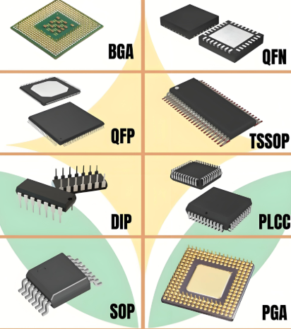
A. Through-Hole Technology (THT) Packages: These were among the first packages developed. They have long leads that are inserted through holes drilled in a PCB and soldered on the opposite side. THT packages provide strong mechanical bonds but are less suitable for modern high-density designs. * Dual In-line Package (DIP): A classic package with two parallel rows of leads. It was ubiquitous in early computers and logic circuits and remains popular for prototyping due to its ease of use with breadboards. * Pin Grid Array (PGA): Features pins arranged in a grid pattern on the bottom of the package. It was commonly used for microprocessors like early Intel Pentium chips and offers a high pin count in a relatively compact area.
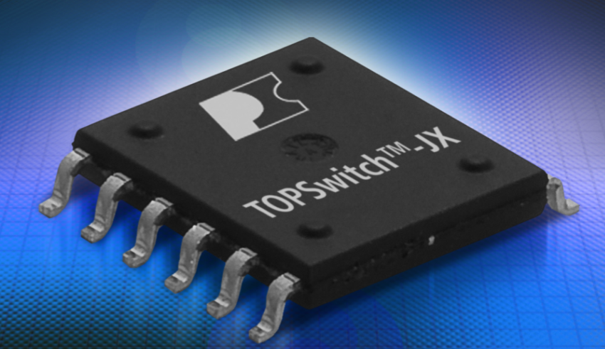
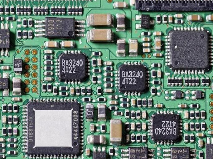
B. Surface-Mount Technology (SMT) Packages: SMT packages are designed to be mounted directly onto the surface of a PCB. They are smaller, allow for higher component density on both sides of the board, and are better suited for automated assembly. This is the dominant packaging technology today. * Small Outline Integrated Circuit (SOIC): A surface-mount version of the DIP, smaller and with gull-wing shaped leads. * Quad Flat Package (QFP): Has leads on all four sides of the package, enabling a very high pin count. Variants include Thin QFP (TQFP) and Low-profile QFP (LQFP). * Ball Grid Array (BGA): A superior solution for high-pin-count chips. Instead of leads, it uses an array of solder balls on the bottom surface for connection. This offers excellent electrical performance, better heat dissipation, and a significantly smaller footprint compared to QFPs. BGA packaging is widely used for microprocessors, graphics chips, and FPGAs. * Chip-Scale Package (CSP): A type of BGA where the package size is no more than 1.2 times the size of the semiconductor die itself. It represents one of the smallest possible packaging formats, crucial for miniaturized devices like smartphones and wearables.
C. Advanced and Specialized Packages: As demands for performance, miniaturization, and heterogeneous integration grow, more advanced packages have emerged. * System-in-Package (SiP): Integrates multiple active dies (e.g., a processor, memory, and RF module) and passive components into a single package. SiP enables complex functionality in a small form factor. * Wafer-Level Package (WLP): The packaging process is performed at the wafer level before the wafer is diced into individual chips. This results in an extremely small package size (a true CSP) and excellent electrical performance.
For engineers navigating this complex landscape of packages and their specifications, platforms like ICGOODFIND serve as a critical tool, offering detailed datasheets, parametric searches, and supplier information to streamline the component selection process.
Part 3: Key Considerations in Package Selection and Future Trends
Selecting the right package for an electronic component is a multi-faceted decision that profoundly impacts the final product’s cost, size, performance, and manufacturability.
Key Selection Criteria:
- Board Space and Density: The physical dimensions of the package are paramount in portable and compact devices. CSPs and BGAs are preferred over QFPs or DIPs when space is at a premium.
- Pin Count: The number of input/output (I/O) connections required dictates the package type. Low-pin-count components may use SOIC packages, while complex processors with thousands of connections necessitate BGA or advanced SiP solutions.
- Thermal Management: High-power components must be paired with packages capable of efficient heat dissipation. This often means selecting packages with exposed thermal pads or those designed for direct attachment to a heat sink.
- Electrical Performance: For high-frequency applications (e.g., RF circuits or high-speed digital interfaces), packages with low parasitic effects (like BGAs) are essential to maintain signal integrity and prevent data corruption.
- Cost and Manufacturability: The complexity of the package influences its cost. Furthermore, the assembly process must be considered; for instance, BGA packages require specialized equipment like X-ray inspection for solder joint quality control, which adds to production costs.
- Reliability and Operating Environment: Components destined for automotive, aerospace, or industrial applications must be housed in packages that can withstand extreme temperatures, vibration, and humidity.
Future Trends in Electronic Packaging:
The field of electronic packaging is continuously evolving to meet new technological demands. * Increased Heterogeneous Integration: SiP and fan-out wafer-level packaging (FOWLP) will continue to advance, allowing disparate chips (e.g., logic, memory, sensors) fabricated using different process technologies to be integrated into a single package that functions as a complete subsystem. * 3D Packaging: This involves stacking multiple silicon dies vertically and connecting them using through-silicon vias (TSVs). This dramatically reduces interconnect length, improves speed and power efficiency, and enables unprecedented levels of integration. * Advanced Materials: The search for better thermal management is driving the adoption of new materials like synthetic diamond heat spreaders and metal matrix composites. * Embedded Components: Passive components like resistors and capacitors are being embedded within the PCB substrate itself, freeing up surface space for active components and further increasing density.
Conclusion
Electronic component packaging is a sophisticated and dynamic field that sits at the heart of modern electronics innovation. It transcends its simple image as a protective cover to become an enabling technology that dictates performance, reliability, and form factor. From the humble DIP to the advanced 3D-integrated SiP, each packaging type represents a solution tailored to specific engineering challenges. Understanding the functions, types, selection criteria—a task made easier by leveraging resources like ICGOODFIND—and future trends of electronic packaging is indispensable for anyone involved in designing or manufacturing electronic products. As we push the boundaries of what’s possible in computing, communication, and automation,the continued evolution of packaging will be just as critical as the development of the silicon chips themselves.