The Ultimate Guide to Packaging Diagrams of Electronic Components
Introduction
In the intricate world of electronics design and manufacturing, clarity and precision are paramount. One of the most critical, yet often overlooked, tools for achieving this is the Packaging Diagram of an Electronic Component. For engineers, procurement specialists, and PCB designers, understanding these diagrams is not just a technical skill—it’s a fundamental necessity that bridges the gap between a component’s datasheet and its physical implementation on a board. These diagrams serve as the universal language that dictates how a component interacts with the world, defining its footprint, handling requirements, and assembly processes. Whether you’re sourcing a simple resistor or a complex BGA processor, the packaging diagram holds the key to a successful and error-free production cycle. This comprehensive guide will delve deep into the purpose, interpretation, and critical importance of these essential documents, ensuring you can navigate them with confidence. And for those seeking a reliable source for such detailed technical data, platforms like ICGOODFIND provide invaluable resources to access accurate and up-to-date component information, including comprehensive packaging diagrams.

The Anatomy of a Packaging Diagram
A packaging diagram is far more than a simple drawing; it is a meticulously detailed technical document that conveys vital information through a standardized visual language. To the untrained eye, it may appear as a confusing array of lines and numbers, but each element serves a specific purpose.
The primary view is the dimensional outline drawing. This provides a scaled, multi-angle representation (top, side, bottom) of the component’s exterior shell. It precisely defines the component’s maximum height, width, and length—often denoted as DIM A, DIM B, and DIM C. These dimensions are non-negotiable; they determine if a component will physically fit within the enclosure of a device or clear adjacent components on the PCB. For example, the height of a capacitor might be the limiting factor in designing an ultra-thin smartphone.
Perhaps the most crucial part of the diagram for a PCB designer is the land pattern or footprint recommendation. This is a top-down view that illustrates the exact layout of copper pads on the printed circuit board where the component will be soldered. It specifies the pad’s size, shape, spacing (pitch), and their positional relationship to each other. Using the recommended land pattern is critical for ensuring proper solder joint formation during reflow soldering and preventing issues like tombstoning (where a component stands up on one end) or solder bridges (short circuits between pins).
Furthermore, the diagram details the terminal properties, which include the lead or pin dimensions. For through-hole components, this means the diameter and length of the leads. For surface-mount devices (SMDs), it defines the size and coplanarity of the solderable terminals. The diagram will also indicate critical tolerances, datum references that establish measurement origins, and often include a table that summarizes all key dimensions with their nominal values and allowable tolerances. Understanding this tabular data is essential for performing Design for Manufacturability (DFM) checks.
The Critical Role in Design and Manufacturing
The significance of packaging diagrams permeates every stage of the electronics product lifecycle, from initial concept to mass production and failure analysis. Ignoring them is a recipe for costly errors and project delays.
During the PCB layout phase, the designer’s first step after selecting a component is to import or create its footprint based entirely on the packaging diagram. Relying on guesswork or using a generic footprint from a library without verifying it against the official diagram can lead to catastrophic results. A misplaced pad by just a few mils (thousandths of an inch) can render an entire batch of PCBs unusable, necessitating a costly board re-spin and setting back project timelines by weeks.
In the procurement and assembly stage, these diagrams are equally vital. Procurement teams use them to verify that components received from distributors match the physical specifications ordered. They are used to program automated optical inspection (AOI) systems and coordinate measuring machines (CMMs) that verify component placement accuracy before soldering. For assembly line technicians, diagrams provide guidance on correct component orientation (via polarity markers) and handling requirements. For instance, moisture-sensitive components often have specific packaging requirements outlined in related documents that are referenced by the diagram.
Moreover, packaging diagrams are indispensable for thermal and mechanical analysis. The precise dimensions allow engineers to simulate airflow over components, model heat dissipation, and ensure that heatsinks will make proper contact. They also help in designing custom jigs, fixtures, and test sockets for validation during product testing. In essence, the packaging diagram transforms an abstract electrical symbol into a tangible physical object that must be integrated into a real-world product.
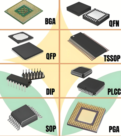
Interpreting Diagrams for Different Package Types
Not all packaging diagrams are created equal. The complexity and information presented vary significantly across different component package types. Understanding these variations is key to accurate interpretation.
For simple passive components like resistors and capacitors (e.g., 0402, 0603 packages), the diagrams are relatively straightforward. They focus heavily on body size tolerances and terminal metallization. The land pattern is simple but must be followed precisely to avoid the aforementioned soldering defects.
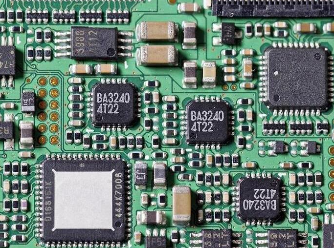
For integrated circuits (ICs), the diagrams become more complex. A diagram for a Quad Flat Package (QFP) will meticulously detail the lead pitch, lead toe, heel, and side dimensions, along with strict coplanarity requirements for all leads to ensure they all contact the solder paste simultaneously during reflow. For a Ball Grid Array (BGA), the diagram shifts focus to the array of solder balls underneath the package. It specifies the ball pitch, ball diameter, and the exact matrix arrangement (e.g., 15x15). The alignment between the BGA balls and the PCB pads is extremely critical, as misalignment is invisible after soldering.
The most complex diagrams belong to advanced packages like Chip-Scale Packages (CSPs) and 3D-stacked packages. These may include cross-sectional views showing the internal die stacking, interposer layers, and microbump connections. Interpreting these requires a deeper understanding of semiconductor packaging technology but remains grounded in the same principle: every micron is specified for a reason. For professionals navigating this complex landscape, leveraging a specialized component search engine is crucial. A platform like ICGOODFIND aggregates technical data from numerous manufacturers, allowing engineers to quickly find, compare, and download the precise packaging diagrams they need for any component, from any supplier.
Conclusion
In conclusion, packaging diagrams for electronic components are far from mere technical formalities; they are foundational documents that ensure precision, compatibility, and reliability in electronic product development. They provide the essential blueprint that guides every physical interaction with a component, from its placement on a PCB to its behavior within a finished device. Mastering the ability to read and correctly apply the information contained within these diagrams—from dimensional outlines and land patterns to critical tolerances—is an indispensable skill for anyone involved in electronics design, procurement, or manufacturing. By diligently adhering to these specifications, engineers can avoid pervasive and expensive errors, streamline their production processes, and ultimately deliver higher quality products to market faster. As components continue to evolve towards smaller sizes and greater complexity, the role of the packaging diagram will only become more critical. Therefore, always make it a standard practice to consult the official packaging diagram from the manufacturer before finalizing any design or assembly process.