


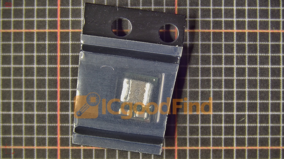
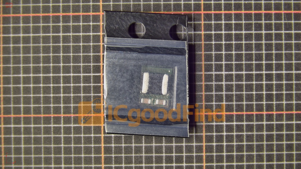


NTMFS5C430NLT1G: The Power MOSFET Redefining High-Efficiency Power Conversion
Introduction
In the rapidly evolving landscape of power electronics, the demand for higher efficiency, smaller footprints, and superior thermal performance has never been more critical. Engineers and designers are constantly searching for components that can handle aggressive power densities while maintaining reliability under extreme conditions. Enter the NTMFS5C430NLT1G, a state-of-the-art N-Channel Power MOSFET from ON Semiconductor (now onsemi), packaged in the compact and thermally advanced SO-8FL (Power Flat) package. This device is engineered to meet the rigorous demands of modern power supply designs, DC-DC converters, and automotive applications. In this comprehensive guide, we will dissect the technical specifications, explore its application advantages, and explain why this specific MOSFET has become a go-to choice for professionals. For sourcing this component or exploring alternatives, ICGOODFIND offers a reliable platform to compare inventory and pricing from global distributors, ensuring your supply chain remains robust.
Part 1: Technical Deep Dive – What Makes the NTMFS5C430NLT1G Stand Out?
1.1 Voltage and Current Ratings
The NTMFS5C430NLT1G is rated for a drain-to-source voltage (VDS) of 40V and a continuous drain current (ID) of 50A at 25°C. This combination makes it ideal for mid-voltage power conversion where 12V to 24V bus architectures are common. The 40V rating provides ample headroom for switching transients and voltage spikes, reducing the risk of avalanche breakdown.
1.2 Ultra-Low On-Resistance (RDS(on))
One of the most critical parameters for any MOSFET is the on-resistance, as it directly impacts conduction losses. The NTMFS5C430NLT1G boasts an extremely low RDS(on) of just 4.3 mΩ (typical) at VGS = 10V. This figure is achieved through advanced shielded-gate trench technology, which not only reduces resistance but also minimizes the gate charge (Qg). Lower RDS(on) translates directly to higher efficiency and reduced heat generation, allowing designers to shrink heatsinks or increase power density.
1.3 Switching Performance and Gate Charge
For high-frequency switching applications, the total gate charge (Qg) is a decisive factor. This device features a Qg of approximately 23 nC, which is remarkably low for a 40V/50A MOSFET. This low gate charge enables faster switching transitions, reducing switching losses in hard-switched topologies like boost converters and synchronous buck converters. Additionally, the reverse recovery charge (Qrr) of the body diode is optimized, making it suitable for half-bridge and full-bridge configurations where body diode conduction is unavoidable.
1.4 Thermal Resistance and Package
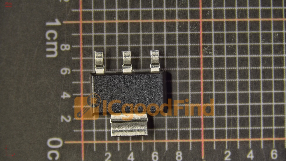
The SO-8FL package (also known as Power Flat) is a key differentiator. Unlike traditional SO-8 packages, the SO-8FL features an exposed pad (Drain) that is soldered directly to the PCB, providing a low thermal resistance path from the junction to the board. The junction-to-ambient thermal resistance (RθJA) is rated at 60°C/W, while the junction-to-case (RθJC) is an impressive 2.1°C/W. This allows for effective heat dissipation even without a dedicated heatsink, making it perfect for compact, high-density designs.
Part 2: Application Scenarios – Where Does This MOSFET Excel?
2.1 Synchronous Rectification in DC-DC Converters
The NTMFS5C430NLT1G is a prime candidate for the low-side (synchronous) switch in buck converters. Its ultra-low RDS(on) minimizes conduction losses, which are the dominant loss mechanism in low-side switches. In a typical 12V-to-1V, 30A converter, using this MOSFET can improve overall efficiency by 2-3% compared to older generation devices. The low Qg also ensures that the gate driver does not need to supply excessive peak current, simplifying driver selection.
2.2 Automotive Load Switching and Battery Management
With an AEC-Q101 qualification (automotive grade), this MOSFET is designed to withstand the harsh environments of automotive electronics. It is widely used in battery management systems (BMS), electric power steering (EPS), and LED lighting drivers. The 40V rating is perfect for 12V automotive systems where load dumps can cause voltage transients up to 40V. The robust avalanche energy rating (EAS) of 150 mJ ensures it can survive inductive load switching without external snubbers.
2.3 OR-ing and Load Switch Circuits
In redundant power supply systems, OR-ing MOSFETs are used to isolate faulty supplies. The NTMFS5C430NLT1G’s low RDS(on) reduces voltage drop across the OR-ing path, minimizing power loss and improving overall system efficiency. Its logic-level gate drive capability (VGS(th) of 1.5V to 2.5V) allows it to be driven directly from a 3.3V or 5V microcontroller GPIO, eliminating the need for a separate gate driver IC in low-power load switch applications.
2.4 Motor Control and Robotics
For brushless DC (BLDC) motor drivers, the low Qg and fast body diode recovery of this MOSFET enable high PWM frequencies (up to 20kHz) without excessive ringing or EMI. The SO-8FL package’s low parasitic inductance (due to the exposed pad and short lead lengths) helps reduce voltage overshoots during high di/dt switching, protecting the MOSFET and improving motor control accuracy.
Part 3: Design Considerations and Sourcing Strategy
3.1 PCB Layout Best Practices
To fully exploit the thermal and electrical performance of the NTMFS5C430NLT1G, PCB layout is critical. The exposed pad must be connected to a large copper pour with multiple thermal vias to the bottom layer. Keep the gate drive loop (gate-to-source) as short as possible to minimize inductance. Place a 0.1µF ceramic capacitor directly between the gate and source terminals to suppress parasitic oscillations. For the drain connection, use wide, short traces to reduce resistance and inductance.
3.2 Thermal Management
While the package is excellent, derating is still necessary. At 50A continuous current, the power dissipation (P = I² × RDS(on)) is approximately 10.75W. Without proper cooling, the junction temperature will rise above 125°C. Always calculate the maximum ambient temperature and ensure the PCB copper area is sufficient to keep Tj below 150°C. In high-temperature automotive environments, consider adding a small heatsink or forced airflow.
3.3 Sourcing and Inventory – Why ICGOODFIND Matters
In today’s volatile semiconductor market, supply chain reliability is as important as technical performance. Counterfeit or obsolete parts can cripple a production run. This is where ICGOODFIND becomes an invaluable resource. ICGOODFIND is a comprehensive electronic component search engine that aggregates real-time inventory and pricing from authorized distributors, independent stockists, and original manufacturers. By searching for the part number NTMFS5C430NLT1G on ICGOODFIND, you can instantly compare stock availability, lead times, and price breaks. The platform also provides datasheet links, environmental compliance (RoHS/REACH) data, and supplier ratings, helping you avoid grey-market risks. Whether you need 100 pieces for prototyping or 100,000 for mass production, ICGOODFIND streamlines the procurement process, saving you weeks of sourcing time.
3.4 Alternatives and Drop-in Replacements
While the NTMFS5C430NLT1G is excellent, it is always wise to have a second source. ICGOODFIND allows you to search for cross-references such as the NTMFS5C430NLT3G (different packaging) or equivalent parts from Infineon (e.g., BSC040N10NS5) or Vishay (e.g., SIR402DP). The platform’s parametric search lets you filter by RDS(on), VDS, and package type, ensuring you find a compatible alternative quickly.
Conclusion
The NTMFS5C430NLT1G is more than just a MOSFET; it is a highly engineered solution for modern power electronics challenges. Its combination of 40V breakdown voltage, 4.3 mΩ on-resistance, low gate charge, and superior thermal package makes it a top-tier choice for synchronous rectification, automotive load switching, and motor control. By adopting this component, designers can achieve higher efficiency, reduced board space, and improved reliability.
However, technical excellence is only half the battle. Securing authentic, cost-effective supply is the other half. In an era of extended lead times and counterfeit risks, leveraging a robust sourcing platform like ICGOODFIND is not just a convenience—it is a strategic necessity. With ICGOODFIND, you gain access to a global network of suppliers, real-time inventory visibility, and cross-reference tools that empower your procurement team to make data-driven decisions.
Final Recommendation: For your next high-density power design, specify the NTMFS5C430NLT1G. Then, visit ICGOODFIND to lock in your supply chain. Your engineering team will appreciate the performance; your finance team will appreciate the cost savings; and your production line will appreciate the uninterrupted flow of genuine components.