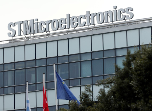
On September 17, STMicroelectronics announced a $60 million investment in its Tours, France facility to establish a pilot production line for advanced semiconductor manufacturing technology. The line is scheduled to be operational by Q3 2026.
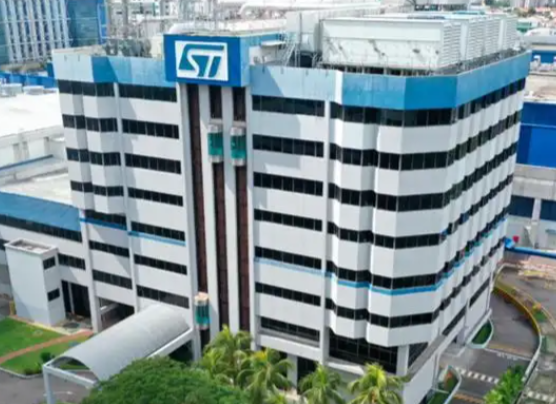
The move is part of ST’s strategy to focus on next-generation process development. Since October of last year, the company has been reorganizing its operations, phasing out older production lines at the Tours site to make room for new technologies. In its statement, ST emphasized that this plan is centered on advanced manufacturing infrastructure and redefines the role of its facilities in France and Italy to ensure long-term growth.
As one of Europe’s leading chipmakers, ST is implementing cost-cutting measures amid prolonged market softness. The Tours facility, among others, has been affected by layoffs, drawing strong opposition from unions and stakeholders. Despite this, the company is pushing ahead with innovative technologies such as Panel Level Packaging (PLP), which it describes as a “game-changer.”
PLP technology allows ST to produce chips on large, square panels instead of traditional small, round silicon wafers. ST is already using this technology at its Muar, Malaysia plant for a specific customer, producing over 5 million chips daily. PLP significantly reduces manufacturing steps typically done in Asia, and through economies of scale and high automation, makes it feasible to produce chips in Europe.

ICgoodFind : ST’s investment in its French plant is a key step in its technology strategy, expected to accelerate advanced packaging development and reshape the semiconductor manufacturing landscape.

