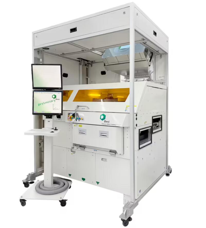
STMicroelectronics has announced a major investment of over €60 million to establish a pilot line for next-generation Panel-Level Packaging (PLP) technology in Tours, France. Scheduled to begin operations in Q3 2026, this initiative aims to advance the adoption of PLP across broader applications while improving efficiency and flexibility.
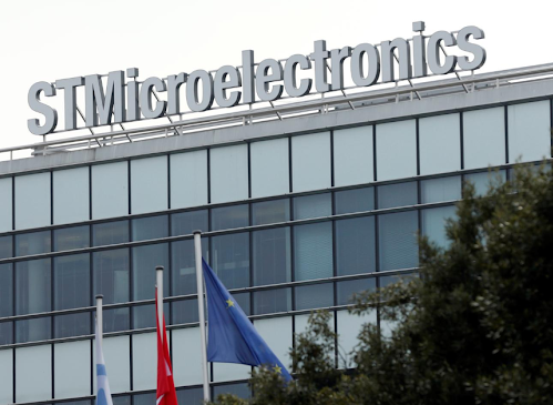
As a key player in advanced PLP technology, STMicroelectronics already operates a highly automated production line using a PLP-DCI variant on 700mm×700mm large panels, achieving a daily output of over 5 million units. This demonstrates the company’s leadership in large-scale panel-level packaging.
Panel-Level Packaging has gained significant attention for its ability to increase chip yield per unit area and deliver substantial cost advantages compared to traditional wafer-level packaging. With growing demand from 5G, AI, and other high-performance applications, STMicroelectronics’ investment positions it at the forefront of advanced packaging innovation.
The new pilot line in Tours will further expand STMicroelectronics’ technological capabilities and provide advanced packaging solutions for demanding sectors such as automotive electronics and industrial controls.
ICgoodFind : This strategic move by STMicroelectronics is set to accelerate the adoption of PLP technology, creating new opportunities for the semiconductor industry.
