Samsung Electronics has dissolved its standalone HBM (High Bandwidth Memory) task force, merging the team and its R&D operations into the existing DRAM design division. This organizational shift signals a move from an emergency response mode to a sustained development phase for its HBM business.
The restructuring is seen as a strategic upgrade, not a retreat. The original team leader remains in charge, and the core talent will continue developing next-generation products like HBM4 and HBM4E. The specialized task force was initially formed in July 2023 to help Samsung catch up with competitor SK Hynix, which then dominated the high-end HBM market.

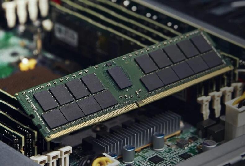
The team delivered significant results, completing core technology verification for HBM4. The new product features a 12-layer stack, bandwidth exceeding 1TB/s—a more than 30% performance gain over mainstream HBM3E—and has achieved stable, mass-production-ready yields. Crucially, Samsung has enabled technological synergy between HBM and DRAM, allowing its modified 1αnm DRAM production line to manufacture HBM, significantly cutting costs.
This integration is a logical step. As a high-end extension of DRAM, HBM shares synergies in materials, packaging, and processes. Being part of the DRAM division allows HBM R&D to leverage mature supply chains, testing equipment, and established customer channels.
The global HBM market is on the verge of explosive growth, projected to reach $45 billion in 2025. Samsung's reorganization positions it to compete more effectively in the upcoming HBM4 mass-production race.
ICgoodFind: This move reflects HBM's maturation into a mainstream technology, where intensified competition will drive faster performance gains and cost efficiencies.
