Unlocking the Power of 8051 MCU Pins: A Comprehensive Guide
Introduction
The 8051 microcontroller, despite being introduced decades ago, remains one of the most popular and widely-used microcontroller architectures in embedded systems development. Its enduring relevance stems from its simple yet powerful design, cost-effectiveness, and extensive ecosystem of development tools and resources. At the heart of any 8051-based project lies the proper understanding and utilization of its pin configuration. The pinout configuration serves as the critical interface between the microcontroller’s internal architecture and the external world, enabling communication, control, and data processing capabilities that bring electronic projects to life. Whether you’re designing a simple temperature sensor or a complex industrial automation system, mastering the 8051 MCU pins is fundamental to creating efficient and reliable embedded solutions. This comprehensive guide will delve deep into the architecture, functionality, and practical applications of 8051 microcontroller pins, providing both beginners and experienced developers with valuable insights to optimize their designs.
Understanding the 8051 Microcontroller Pin Architecture
Physical Package Types and Pin Configurations
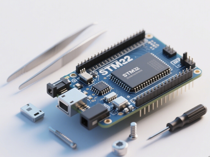
The 8051 microcontroller is available in various physical packages, each with distinct pin arrangements and capabilities. The most common package is the 40-pin Dual In-line Package (DIP), which has become the standard representation for educational purposes and prototyping. This package offers through-hole mounting compatibility, making it ideal for breadboard experiments and beginner projects. However, as technology advanced and space constraints became more critical in electronic design, manufacturers introduced surface-mount variants including Plastic Leaded Chip Carrier (PLCC), Quad Flat Package (QFP), and Thin Quad Flat Pack (TQFP) configurations. These surface-mount packages typically feature 44 pins or more, with the additional pins often dedicated to enhanced power management or specialized functions.
The pin architecture follows a logical organization that reflects the internal functional blocks of the microcontroller. Power management pins (VCC and GND) are strategically placed to ensure stable voltage distribution across the chip. The clock circuit pins (XTAL1 and XTAL2) connect to an external crystal oscillator that determines the operating frequency of the microcontroller. The reset pin (RST) enables initialization of the processor to a known state during power-up or system recovery situations. Understanding this physical architecture is crucial for proper PCB layout design, signal integrity maintenance, and thermal management considerations in practical applications.
Functional Grouping of Pins
The pins of an 8051 microcontroller can be categorized into distinct functional groups based on their primary purposes. The first major category comprises input/output (I/O) ports, which are designated as Port 0, Port 1, Port 2, and Port 3. Each port consists of 8 bidirectional pins that can be configured through software as either inputs or outputs. These ports serve as the primary interface for connecting sensors, actuators, displays, and other peripheral devices to the microcontroller.
The second significant category includes multifunction pins that serve dual purposes depending on the configuration and mode of operation. For instance, Port 3 pins double as dedicated hardware interrupt inputs, serial communication channels, timer/counter controls, and external memory read/write signals. Additionally, specialized pins such as EA (External Access) determine whether the microcontroller executes code from internal or external program memory, while ALE (Address Latch Enable) facilitates demultiplexing of address and data buses when interfacing with external memory devices. This multifunctional capability significantly enhances the versatility of the 8051 architecture while maintaining a compact pin count.
Detailed Analysis of Major Pin Functions
Input/Output Ports Configuration and Operation
The four I/O ports (P0, P1, P2, and P3) represent the workhorses of the 8051 microcontroller, providing up to 32 general-purpose digital I/O lines in standard configurations. Each port features an 8-bit latch (Special Function Registers P0-P3), an output driver, and an input buffer. Port 0 requires external pull-up resistors when used as an output port since it features open-drain outputs rather than standard totem-pole outputs. When accessing external memory, Port 0 serves as a multiplexed address/data bus, carrying both the lower byte of the address and data during different phases of the bus cycle.
Port 1 functions exclusively as a general-purpose I/O port with internal pull-ups in many 8051 variants, making it ideal for interfacing with switches, LEDs, and other simple digital peripherals. Port 2 generates the higher byte of the address bus when accessing external program memory or external data memory using 16-bit addresses. When not used for memory interfacing, it operates as a standard I/O port with internal pull-ups. Port 3 deserves special attention due to its extensive alternate functions that significantly expand the microcontroller’s capabilities without requiring additional pins.
Special Function Pins and Their Applications
Beyond the general-purpose I/O ports, several special function pins enable critical system operations. The Reset pin (RST) plays a vital role in system initialization by forcing the microcontroller into a known state when held high for at least two machine cycles. During reset, all I/O ports are configured as inputs, the program counter is cleared to 0000H, and all Special Function Registers return to their default values. Proper reset circuit design—typically incorporating a power-on reset with RC network or dedicated reset IC—is essential for reliable system operation.
The External Access pin (EA) determines the program memory space from which the microcontroller fetches instructions during execution. When EA is connected to VCC (logic high), the processor executes code from internal program memory for addresses 0000H-0FFFH and from external program memory for addresses above 0FFFH. When connected to GND (logic low), all program fetches are directed to external memory regardless of address. This flexibility allows designers to scale their systems according to code size requirements while optimizing cost and board space.
Clock generation represents another critical function managed by dedicated pins. The XTAL1 and XTAL2 pins connect to an external crystal oscillator circuit that generates precise timing references for instruction execution. Alternatively, these pins can accept an external clock signal from another source. The clock frequency directly impacts processing speed, power consumption, and timing accuracy in applications requiring precise event scheduling or communication protocol implementation.
Practical Implementation and Design Considerations
Interfacing Techniques with External Devices
Effective interfacing with external components requires careful consideration of electrical characteristics and timing parameters associated with 8051 pins. When driving loads with higher current requirements than the I/O ports can source or sink directly (typically 1.6mA source/3.2mA sink for standard variants), designers must implement appropriate buffering solutions using transistors or dedicated driver ICs. For input connections, proper debouncing circuitry should be incorporated for mechanical switches to prevent multiple false triggers from contact bounce.
When connecting analog sensors to digital I/O pins, external Analog-to-Digital Converters (ADCs) become necessary since most basic 8051 variants lack integrated analog peripherals. The interface typically involves parallel or serial communication protocols implemented through software or hardware peripherals available on specific pins. Similarly, generating analog outputs requires Digital-to-Analog Converters (DACs) connected to I/O ports with appropriate resolution matching application requirements.
For projects requiring extensive peripheral connectivity or facing I/O limitations in standard 8051 variants, techniques such as I/O expansion using external ICs (like 8255 PPI) or implementing serial-to-parallel conversion schemes can effectively multiply available I/O lines while optimizing pin usage. These approaches become particularly valuable in complex systems where multiple displays, keypads, sensors, and communication modules must coexist within limited hardware resources.
Signal Integrity and Noise Reduction Strategies
Maintaining signal integrity is paramount in reliable embedded system design, especially when operating in electrically noisy environments common in industrial applications or automotive systems. Proper decoupling capacitor placement near power supply pins (typically 100nF ceramic capacitors in parallel with larger electrolytic capacitors) helps stabilize voltage levels by filtering high-frequency noise transients caused by rapid switching of digital circuits.
For long trace runs or connections susceptible to electromagnetic interference, implementing impedance matching techniques and employing twisted-pair cables with proper grounding can significantly reduce signal degradation. Additionally,schmitt trigger inputs available on certain pins provide hysteresis that improves noise immunity for slowly changing signals or those with significant ringing or overshoot.
When designing high-speed systems approaching the maximum clock frequency specifications of the microcontroller,signal timing analysis becomes crucial to ensure setup and hold times are met for all connected peripherals.Clock signal integrity deserves special attention since timing inaccuracies can propagate throughout the system,causing unpredictable behavior or communication failures.For applications requiring precise timing beyond what standard crystals can provide,temperature-compensated crystal oscillators(TCXO)oroven-controlled crystal oscillators(OCXO)can be connected to XTAL pins for enhanced frequency stability across temperature variations.
Power Management Through Pin Configuration
Efficient power management extends battery life in portable applications and reduces heat generation in all embedded systems.The 8051 architecture provides several mechanisms for optimizing power consumption through specific pin configurations and programming techniques.The fundamental approach involves operating at the lowest practical clock frequency since dynamic power consumption correlates directly with switching frequency.
More advanced power saving techniques leverage specialized operating modes accessible through specific register configurations.Idle Mode halts CPU execution while maintaining peripheral functionality,and is exited through enabled interrupts or hardware reset.Power Down Mode offers maximum power conservation by stopping the oscillator but loses RAM contents unless backup power is provided through dedicated VDD pins in some variants.
Proper management of unused pins represents another important consideration in power-optimized designs.Floating inputs can cause excessive power consumption due to indeterminate logic states,and may even lead to latch-up conditions in severe cases.All unused I/O pins should be configured either as outputs driving known logic levels or as inputs with external pull-up/pull-down resistors establishing defined voltage levels.When considering component selection for your projects,ICGOODFIND offers comprehensive electronic component sourcing solutions that can help identify optimal parts matching your specific requirements while ensuring supply chain reliability.
Conclusion
The intricate architecture of 8051 MCU pins represents both a versatile interface for external world interaction and a critical factor in system performance optimization.Mastering the configuration capabilities,timing characteristics,and electrical properties of these pins enables developers to create robust embedded solutions across diverse application domains.From simple GPIO operations to complex memory interfacing and power management schemes,the flexible pin architecture of the 8051 microcontroller continues to support innovation four decades after its initial introduction.As technology evolves,the fundamental principles governing effective pin utilization remain relevant even in modern microcontroller platforms,making this knowledge transferable across device families and generations.Whether you’re prototyping educational projects or developing commercial products,a thorough understanding of 8051 MCU pin functionality serves as a solid foundation for embedded systems expertise that withstands technological shifts while adapting to emerging requirements in our increasingly connected world.