Semiconductor packaging leader Amkor Technology has launched construction of a $7 billion packaging and testing campus in Arizona, set to become the first large-scale advanced packaging facility in the United States. The site is scheduled to begin operations in early 2028.

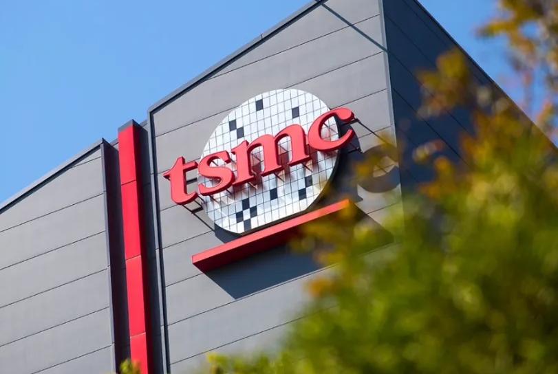
Supported by the US CHIPS Act and local incentives, the project will feature over 750,000 square feet of cleanroom space and is expected to create 3,000 high-skilled jobs. Located near TSMC’s wafer fab, the campus will help establish an end-to-end domestic semiconductor manufacturing ecosystem, serving leading clients such as Apple and NVIDIA.
Amkor’s CEO described the investment as a strategic step to meet cutting-edge customer demand for advanced packaging while strengthening U.S. semiconductor infrastructure.
ICgoodFind : Advanced packaging is emerging as a strategic focus in global supply chains, with localization accelerating and requiring close industry attention.


