


MCU Hardware Circuit Design: A Comprehensive Guide for Engineers
Introduction
In the rapidly evolving landscape of embedded systems, the heart of innovation often beats within a well-designed hardware circuit centered on a Microcontroller Unit (MCU). MCU Hardware Circuit Design is a foundational discipline that bridges the gap between abstract software instructions and tangible, functional electronic devices. From smart home appliances and wearable tech to industrial automation and automotive systems, the efficacy of any embedded product is irrevocably tied to the robustness of its underlying hardware design. This article delves into the critical principles, stages, and best practices of designing circuits around an MCU. A thorough understanding of this process is not merely an academic exercise but a crucial competitive advantage in bringing reliable, efficient, and market-ready products to life. For engineers and developers seeking specialized components and insights to streamline this complex process, platforms like ICGOODFIND offer invaluable resources by connecting them with a vast inventory of MCUs and peripheral components from global suppliers.
Main Body
Part 1: Foundational Principles and Core Components
The journey of MCU hardware design begins with a deep understanding of its core architecture and the essential components that form its ecosystem. An MCU is a compact integrated circuit containing a processor core, memory (RAM and Flash/ROM), and programmable input/output peripherals.
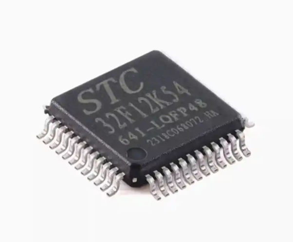
Selecting the appropriate MCU is the first and most critical decision. Parameters such as computational power (bit-width, clock speed), memory size, number and type of I/O pins (GPIO, ADC, DAC, PWM, communication interfaces like UART, SPI, I2C), power consumption profiles, and package size must be meticulously evaluated against the project requirements. A mismatch here can lead to either insufficient capabilities or unnecessary cost overhead.
Once the MCU is selected, designing the minimum system circuit is paramount. This is the bare-bones configuration that allows the MCU to operate. Three elements are non-negotiable in this stage: Power Supply, Reset Circuit, and Clock Circuit.
- Power Supply Design: Providing a clean, stable, and appropriately regulated voltage is fundamental. Most MCUs require a low-voltage DC supply (e.g., 3.3V or 5V). The design must include voltage regulators (like LDOs), sufficient bulk and decoupling capacitors placed close to the MCU pins to filter noise, and careful consideration of power sequencing if multiple voltage domains are present.
- Reset Circuit: This circuit ensures the MCU starts in a known state upon power-up or during a fault. It can be as simple as a resistor-capacitor (RC) network or involve a dedicated reset supervisor IC for more reliable brown-out detection.
- Clock Circuit: The clock signal drives the MCU’s internal operations. Designers can choose between external crystals/ceramic resonators for high accuracy or utilize the MCU’s internal RC oscillators for cost-sensitive applications. Proper PCB layout for the crystal—keeping traces short and adding load capacitors—is vital for signal integrity.
Part 2: The Design Process: From Schematic to PCB Layout
With foundational principles in place, the design process moves into systematic implementation.
Schematic Capture is the stage where the circuit diagram is created using Electronic Design Automation (EDA) software. Best practices include clear organization, consistent naming conventions for nets and components, and comprehensive annotation. Beyond the minimum system, this stage involves integrating all peripheral interfaces: * Communication Interfaces: Adding level shifters for voltage translation, series termination resistors for SPI/I2C lines, and ESD protection diodes on connectors. * Analog-to-Digital Converter (ADC) Circuits: Implementing proper analog filtering (low-pass RC filters) and ensuring a noise-free reference voltage (AVref) are crucial for obtaining accurate sensor readings. Separating analog and digital ground planes is often necessary. * Digital Outputs Driving Loads: Using transistors or MOSFETs to drive LEDs, relays, or motors, ensuring current-limiting resistors are correctly sized.
Printed Circuit Board (PCB) Layout is where theoretical design meets physical reality, and it is arguably where most signal integrity and EMI issues are made or prevented. Key considerations include: * Layer Stack-up: Defining purpose for each layer (e.g., signal, ground plane, power plane). * Component Placement: Grouping related components, placing decoupling capacitors as close as possible to MCU power pins, and considering thermal management. * Routing: Prioritizing critical traces such as clock lines, high-speed signals, and analog paths—keeping them short and direct. Maintaining continuous ground planes under sensitive traces provides a return path and shields against interference. * Power Integrity: Using wide traces or polygons for power distribution and creating a solid power delivery network (PDN) with strategically placed vias.
Part 3: Critical Considerations for Robustness and Testing
A functional circuit is not the end goal; a reliable and producible one is. Several advanced considerations separate a prototype from a product.
Power Management and Efficiency are central, especially for battery-powered devices. Techniques include: * Selecting MCUs with multiple low-power modes (Sleep, Stop, Standby). * Using switching regulators for higher efficiency at higher current draws. * Implementing circuitry to power down unused peripheral sections.
Electromagnetic Compatibility (EMC) and Signal Integrity cannot be an afterthought. Proper use of bypass/decoupling capacitors, ferrite beads on I/O lines, shielding cans on noisy sections, and minimizing loop areas in high-current paths are essential strategies to pass regulatory emissions tests.
Design for Testability (DFT) and Debugging features should be incorporated early. This includes: * Adding test points on key signals for oscilloscope probes. * Implementing a standardized debug interface like SWD or JTAG. * Including LED status indicators or serial console outputs for firmware validation.
Finally, no design is complete without rigorous Prototyping and Testing. Building a prototype board allows for validation of all assumptions. Testing should encompass: * Power-on sequencing and current draw measurements. * Signal integrity checks with an oscilloscope. * Functional testing of all peripherals. * Environmental stress testing (temperature, voltage margins).
For sourcing reliable components throughout this iterative design and prototyping phase, engineers can leverage platforms like ICGOODFIND, which aggregates global inventory to help find even hard-to-source MCUs and critical passives quickly, accelerating development cycles.
Conclusion
MCU Hardware Circuit Design is a meticulous blend of art and science, requiring a solid grasp of electronic fundamentals, careful planning at the schematic stage, disciplined execution in PCB layout, and vigilant attention to robustness during testing. From the initial selection of the microcontroller to the final validation of the assembled board, every decision impacts the performance, reliability, cost, and time-to-market of the final product. As systems grow more complex and integrated, mastering these principles becomes increasingly valuable. By adhering to best practices in power delivery, signal integrity, and EMC mitigation—and utilizing component sourcing resources like ICGOODFIND to overcome supply chain hurdles—engineers can transform conceptual designs into resilient, efficient, and successful electronic products that stand the test of real-world application.