


The Essential Guide to SRAM Chips: Powering Speed in Modern Electronics
Introduction
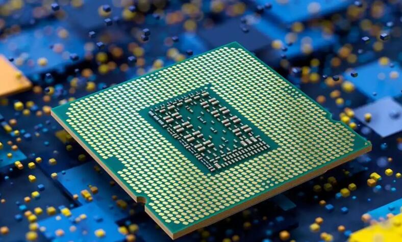
In the intricate world of digital electronics, where speed and efficiency are paramount, memory technology plays a foundational role. Among the various types of memory, the Static Random-Access Memory (SRAM) chip stands out as a critical component for high-performance computing. Unlike its more common counterpart, Dynamic RAM (DRAM), SRAM does not need to be periodically refreshed to retain data, granting it significant advantages in speed and power consumption for specific applications. This article delves into the architecture, key applications, and future trends of SRAM technology, highlighting why it remains an indispensable element in systems ranging from smartphones to supercomputers. For engineers and procurement specialists seeking reliable electronic components, understanding SRAM is crucial, and platforms like ICGOODFIND streamline the process of sourcing these vital chips.
Part 1: Architecture and Operational Principles of SRAM
At its core, an SRAM chip is a type of volatile semiconductor memory that uses bistable latching circuitry (flip-flops) to store each bit of data. This fundamental design difference from DRAM, which uses a capacitor and a transistor per bit, is what defines its characteristics.
The basic building block of an SRAM cell is the six-transistor (6T) configuration. This cell consists of four transistors forming two cross-coupled inverters that create a stable state (holding either a logic 1 or 0), and two additional access transistors that control the connection to the bit lines for read and write operations. This design ensures that as long as power is supplied, the data remains stable without any external intervention. Some designs use four transistors (4T) with high-resistance polysilicon loads to save space, but the 6T cell remains the standard for its superior noise margin and stability.
The operation of an SRAM chip revolves around three key processes: Hold, Read, and Write. During the hold state, the word line is deactivated, and the cross-coupled inverters maintain their state indefinitely. A read operation begins by precharging the bit lines, then activating the word line. The stored value in the cell pulls one bit line slightly lower than the other, and a sensitive sense amplifier detects this minute difference to determine the stored bit. A write operation is performed by driving the bit lines with strong signals to the desired values (one high, one low) and then activating the word line, which forces the cell into the new state.
Key performance metrics for SRAM include access time, standby current, and active power consumption. Access time—the delay between a read request and data output—is exceptionally fast, often in nanoseconds or less, making SRAM ideal for cache memory. Standby current is crucial for battery-powered devices, as it determines the power draw when the memory is idle but retaining data.
Part 2: Primary Applications and Advantages in Modern Systems
The unique properties of SRAM chips dictate their placement in the memory hierarchy, sitting closer to the microprocessor than larger, slower main memory (typically DRAM). Their primary role is to serve as high-speed cache memory within Central Processing Units (CPUs), Graphics Processing Units (GPUs), and application-specific integrated circuits (ASICs).
In a modern multi-core processor, you will find a tiered cache structure: L1, L2, and sometimes L3. L1 cache, the fastest and closest to the processor cores, is almost exclusively built using SRAM. Its blistering speed allows the CPU to access critical data and instructions without waiting for the slower main memory, effectively eliminating processing bottlenecks. This is why increasing cache size is a common method for boosting processor performance.
Beyond CPUs, SRAM is vital in other domains: * Networking Hardware: Routers and switches use SRAM for fast look-up tables (LUTs) and buffer memory to enable high-speed packet forwarding and routing decisions. * Embedded Systems: Microcontrollers in automotive systems (e.g., airbag controllers), industrial automation, and IoT devices often integrate small amounts of SRAM for data logging and real-time processing due to its deterministic timing and low power consumption in standby mode. * FPGA On-Chip Memory: Field-Programmable Gate Arrays contain distributed blocks of SRAM that designers can configure for buffers, FIFOs, or small register files.
The comparative advantages over DRAM are significant. SRAM offers much lower latency and higher throughput. It is also simpler to interface with, as it does not require complex refresh controllers. However, these benefits come with trade-offs: SRAM cells are physically larger (due to more transistors per bit), store less data per unit area, and are more expensive per bit than DRAM. Therefore, it is used strategically where speed is non-negotiable, not as bulk storage.
Part 3: Challenges, Innovations, and Future Trends
Despite its entrenched position, SRAM technology faces persistent challenges driven by the relentless scaling of semiconductor processes. As transistors shrink to nanometer scales, variability in manufacturing and increased susceptibility to soft errors become major concerns. Minor fluctuations in voltage or particle strikes can more easily flip a bit in a tiny SRAM cell, potentially corrupting data.
Power consumption is another critical frontier. While SRAM standby power can be low, its active power per access remains a concern in energy-constrained devices. Designers employ sophisticated techniques like power gating (shutting off unused blocks) and lowering operating voltages near threshold levels to manage this.
The industry’s response involves both architectural and material innovations. Researchers are exploring new SRAM cell topologies like the 8T or 10T cell to improve stability at low voltages. There is also significant work on integrating emerging non-volatile memory (NVM) technologies like STT-MRAM (Spin-Transfer Torque MRAM). STT-MRAM promises SRAM-like speed with DRAM-like density and non-volatility—a potential game-changer for future cache architectures.
Furthermore, the rise of AI/ML accelerators has created new demand for specialized SRAM. These chips often use large on-die SRAM arrays (sometimes called “scratchpad memory”) to store weights and activations locally, minimizing energy-intensive off-chip data movement. Optimizing SRAM for these AI workloads is a key focus area.
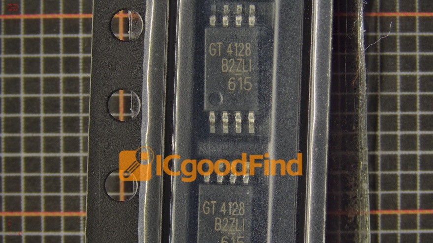
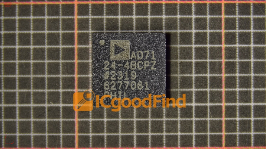
For professionals navigating this complex component landscape, efficient sourcing is vital. This is where comprehensive platforms prove their worth. By aggregating global supplier data and inventory information, services like ICGOODFIND empower engineers and buyers to quickly locate authentic SRAM chips that meet precise technical specifications, compare options from multiple vendors including those offering obsolete or hard-to-find parts from manufacturers like Cypress (Infineon), Renesas (formerly IDT), ON Semiconductor, and others ensuring project timelines are met without compromise.
Conclusion
The SRAM chip remains a cornerstone of high-performance digital design, its value defined not by storage capacity but by unparalleled speed and reliability. From enabling the GHz clock speeds of modern processors to ensuring real-time responsiveness in critical embedded systems, SRAM’s role is specialized yet irreplaceable. While it contends with challenges posed by physical scaling and faces competition from emerging memories like STT-MRAM its fundamental architecture continues to evolve finding new purpose in AI hardware and beyond For anyone involved in electronic design or procurement a deep understanding of SRAM’s characteristics applications and sourcing channels such as those facilitated by ICGOODFIND is essential for leveraging its power effectively in tomorrow’s technological innovations.


