Design of Electronic Components: The Blueprint of Modern Technology
Introduction
In the invisible architecture of our digital world, electronic components serve as the fundamental building blocks. From the smartphone in your pocket to the sophisticated systems controlling satellites in orbit, every piece of modern technology is a symphony of meticulously designed electronic parts. The design of electronic components is not merely a technical process; it is a complex discipline that sits at the intersection of physics, materials science, electrical engineering, and computer-aided design. It is the crucial first step that determines the functionality, efficiency, reliability, and cost of the final electronic product. As technology advances at a breakneck pace, pushing the boundaries of miniaturization and performance, the role of innovative component design becomes increasingly paramount. This article delves into the core principles, the intricate process, and the future trends shaping this critical field, highlighting how platforms like ICGOODFIND are becoming indispensable in navigating the vast ecosystem of component selection and procurement.

The Foundational Principles of Electronic Component Design
The journey of creating a new electronic component is guided by a set of fundamental principles. These are the non-negotiable rules and considerations that engineers must adhere to ensure the component not only works but thrives in its intended application.
1. Functionality and Performance Specifications: Before a single line of a schematic is drawn, designers must have a crystal-clear understanding of what the component needs to do. This involves defining detailed performance specifications: operational voltage and current ranges, frequency response, power dissipation, gain, noise tolerance, and switching speed. For instance, designing a microprocessor for a high-performance server requires a radically different approach than designing a low-power microcontroller for a wearable device. The former prioritizes raw processing speed and parallel computation, often at the expense of power consumption and heat generation. The latter focuses on ultra-low power states, energy efficiency, and minimal leakage current to maximize battery life. This initial specification phase is arguably the most critical, as any oversight here can lead to costly redesigns or a product that fails to meet market needs.
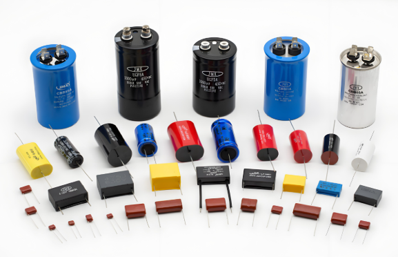
2. Electrical Characteristics and Circuit Theory: At its heart, every electronic component is governed by the laws of circuit theory and electromagnetism. Resistors, capacitors, inductors, transistors, and diodes all have specific electrical behaviors defined by parameters like resistance ®, capacitance ©, and inductance (L). A designer’s deep knowledge of how these parameters interact is essential. For example, when designing a capacitor, one must consider not just its capacitance value, but also its equivalent series resistance (ESR), voltage rating, temperature coefficient, and leakage current. Similarly, transistor design revolves around characteristics such as threshold voltage, transconductance, and breakdown voltage. The interplay between these electrical characteristics dictates the overall behavior of the circuit in which the component will be used. Advanced simulation tools are employed to model these behaviors before physical prototyping, saving immense time and resources.
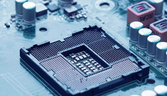
3. Material Science and Selection: The choice of materials is a cornerstone of component design. The properties of the materials used directly influence the component’s performance, durability, and cost. Semiconductors like silicon have been the bedrock of the industry for decades, but new materials like Gallium Nitride (GaN) and Silicon Carbide (SiC) are revolutionizing power electronics with their ability to operate at higher temperatures, voltages, and frequencies with greater efficiency. The substrate upon which integrated circuits (ICs) are built, the metals used for interconnects (like copper or aluminum), and the insulating materials (like silicon dioxide or newer high-k dielectrics) are all selected based on their electrical, thermal, and mechanical properties. The relentless pursuit of Moore’s Law has driven material science to its limits, leading to innovations such as FinFET transistors and exploration into 2D materials like graphene.
4. Thermal Management and Reliability: Electronic components generate heat during operation. If this heat is not effectively managed, it can lead to performance degradation (e.g., “thermal throttling” in processors) or catastrophic failure. Therefore, thermal design is an integral part of the overall component design process. This involves selecting materials with good thermal conductivity, designing physical structures that maximize surface area for heat dissipation (like heat sinks), and incorporating features within ICs to monitor junction temperature. Reliability is another key principle, often quantified as Mean Time Between Failures (MTBF). Designers must ensure components can withstand environmental stresses such as temperature cycling, humidity, vibration, and electrostatic discharge (ESD). Robust design practices, such as implementing ESD protection circuits directly on a chip’s I/O pins, are standard procedure to enhance longevity and ruggedness.
The Electronic Component Design Process: From Concept to Reality
Transforming an abstract idea into a tangible, mass-producible electronic component is a multi-stage process that requires meticulous planning and execution.
1. Schematic Capture and System Definition: The process begins with system-level definition. Engineers outline the block diagram of the entire system, identifying the major functional units and their interconnections. Following this, they move to schematic capture using Electronic Design Automation (EDA) software. Here, the circuit is drawn logically using symbols for various components. This stage defines what the circuit does—the functional relationships between inputs and outputs. It’s a collaborative phase where system architects and circuit designers work together to ensure the schematic meets all the predefined specifications. For integrated circuits, this involves deciding which functions will be implemented in hardware (ASIC) versus software (running on a processor core).
2. Simulation and Modeling: Before committing to expensive fabrication, the proposed design undergoes rigorous simulation. Using tools like SPICE (Simulation Program with Integrated Circuit Emphasis), designers can model the circuit’s behavior under various conditions—different temperatures, supply voltages, and load scenarios. They can analyze DC operating points, transient response (how the circuit behaves over time), AC frequency response, and noise performance. This virtual prototyping phase is indispensable for identifying and rectifying design flaws early. For digital ICs, this extends to Register-Transfer Level (RTL) simulation and verification to ensure logical correctness. For complex analog/RF components, electromagnetic simulation tools are used to model parasitic effects and signal integrity issues that become critical at high frequencies.
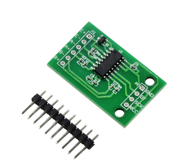
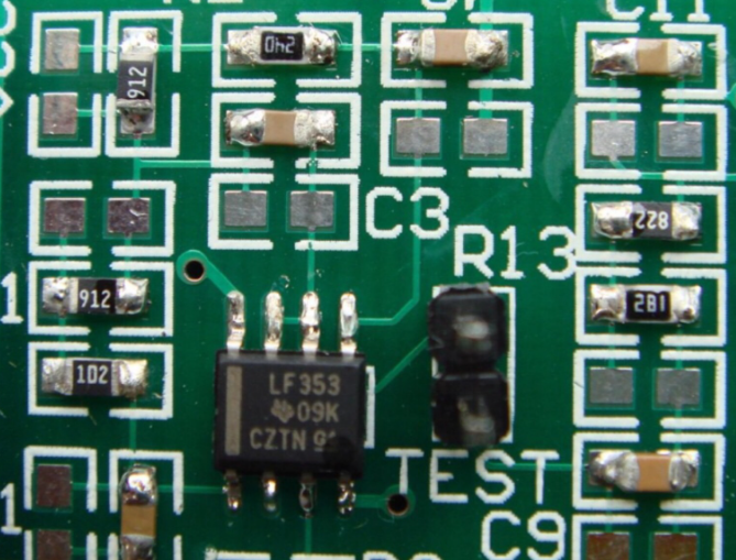
3. Physical Layout Design: Once the schematic is verified through simulation, the physical layout is created. This is where the abstract circuit becomes a geometric representation of masks that will be used in fabrication. For printed circuit boards (PCBs), this involves placing component footprints and routing copper traces between them while adhering to design rules (trace width for current capacity, spacing to prevent crosstalk). For ICs, the layout process is vastly more complex. Designers physically place millions (or billions) of transistors and route interconnects across multiple metal layers in an incredibly dense area. They must contend with parasitic capacitances and resistances, signal propagation delays (timing closure), power distribution networks, and cross-talk between adjacent wires. Design Rule Checking (DRC) and Layout Versus Schematic (LVS) verification are run continuously to ensure the physical layout conforms to the foundry’s manufacturing capabilities and matches the original schematic.
4. Prototyping, Testing, and Validation: After the layout is finalized and verified, it’s sent for fabrication. For ICs, this creates a set of photomasks and runs a small batch through a semiconductor foundry, resulting in “first silicon.” For discrete components or PCBs, initial prototypes are assembled. These prototypes are then put through a gauntlet of tests in laboratory settings. Engineers use oscilloscopes, spectrum analyzers, logic analyzers,and specialized automated test equipment (ATE) to measure every parameter against the original specifications.This phase often uncovers discrepancies between simulatedand real-world performance.Depending on the results,the design may undergo several iterations—a cycle known as “tape-outand spin”—until it meets all requirements for performance,yield,and reliability.
The Future Trajectory and Sourcing with ICGOOFIND
The field of electronic component design is perpetually evolving,directed by powerful marketand technological trends.
1.Miniaturizationand System-on-Chip(SoC): The drive towards smaller,faster,and more power-efficient devices continues.Packaging technologies like System-in-Package(SiP)and 3D-IC stacking are allowing multiple dies(chiplets)to be integrated into a single package,pushing beyondthe scaling limits of traditional SoCs.This “More than Moore” approach enables heterogeneous integration,mixing different process technologies(e.g.,analog,Rf.digital)in one package for optimal performance.
2.The Riseof Al-Hardwareand Specialized ASICs: The explosionof artificial intelligenceand machine learning has createda demandfor specialized processors.Asicand FPGA designis boomingto create hardware accelerators optimizedfor specific Al workloads like tensor operations.Thesedesigns prioritize parallel processing capabilitiesand high-bandwidth memory interfaces over general-purpose computing.
3.Sustainabilityand Eco-Design: Thereis growing pressureto make electronics more sustainable.This influences component design fromthe ground up.Designers are now consideringthe entire lifecycle:using less hazardous materials designingfor energy efficiency during use,and facilitating easier disassemblyand recycling at end-of-life.
In this complex landscape.of constant innovation,findingthe right component fora project can bea daunting task.Thisis where platforms like ICGOODFIND prove invaluable.ICGOODFIND serves asa powerful search engineand information hub for engineersand procurement specialists.It aggregates data from countless suppliers.providing detailed datasheets.inventory availability.pricing comparisons,and lifecycle statusfor millionsof components.Whether you area designer searchingfora drop-in replacement foran obsolete part.or a startup lookingto source cutting-edge sensors.fora new product.ICGOODFIND streamlines.the supply chain discovery process.It helps bridge.the gap between theoretical designand practical implementation ensuringthat brilliant designs can be broughtto life withthe right physical parts.
Conclusion
The designof electronic components isa profound engineering discipline that forms.the bedrockof all modern technology.It isa meticulous journey from abstract conceptto tangible reality.guided by fundamental principlesof electricity.materials science,and physics.The process.involving schematic capture.simulation.layout,and rigorous testing.is both complexand collaborative.As we move forward.the trends of extreme miniaturization.specialized Al hardware,and sustainable design will continue to push designersto new heights of innovation.In this ever-expanding universeof electronic parts.tools like ICGOODFIND empower creators by simplifyingthe critical link between designand procurement ensuringthatthe flowof innovation from mindto market remains uninterrupted.The next time you use an electronic device.takea momentto appreciatethe immense depthof thoughtand design embedded within its smallest parts.