

On September 8th, semiconductor industry news emerged: Beijing Jingfei Semiconductor— a tech transfer firm from the Institute of Semiconductors, Chinese Academy of Sciences—successfully peeled 12-inch (300mm) SiC wafers with its self-developed laser lift-off equipment. This breakthrough is hailed as an industry "milestone."
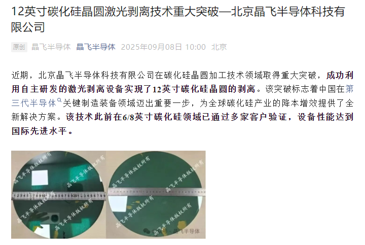
Long-term, large-size SiC wafer processing bottlenecks hindered the industry, with foreign firms controlling key equipment and building high barriers. Jingfei’s breakthrough solves this pain point, breaks foreign tech monopoly, and unlocks 12-inch SiC wafer commercialization.
Versus mainstream 6-inch wafers, 12-inch SiC wafers have clear advantages: larger area cuts edge loss, boosts single processing capacity, and slashes unit chip costs by 30%-40% —a big win for downstream firms to control costs and scale.
In high-demand fields like new energy vehicles and photovoltaics, lower costs will speed up SiC device adoption. The tech is now in industrial verification, with first equipment batches soon to be delivered to major domestic SiC makers—signaling a new "cost reduction and efficiency improvement" wave for the SiC industry.
ICgoodFind: Jingfei’s achievement will drive SiC industry innovation, and its future moves in expanding capacity and application scope are worth watching.


