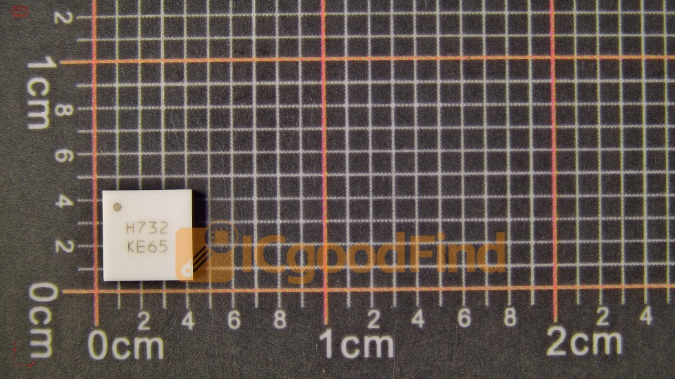


EP4CE15F23C8N: A Comprehensive Guide to the Intel Cyclone IV FPGA
Introduction
In the world of embedded systems, digital signal processing, and high-performance logic design, field-programmable gate arrays (FPGAs) have become indispensable. Among the vast array of FPGA offerings, the EP4CE15F23C8N stands out as a popular choice for engineers seeking a balance between logic density, power efficiency, and cost. This article provides an in-depth exploration of the EP4CE15F23C8N, covering its architecture, key specifications, common applications, and practical design considerations. Whether you are a seasoned FPGA developer or a newcomer evaluating components for your next project, understanding the EP4CE15F23C8N will help you make informed decisions. For sourcing this component or comparing alternatives, resources like ICGOODFIND can streamline your search.
Main Body
Part 1: Architectural Overview and Key Specifications

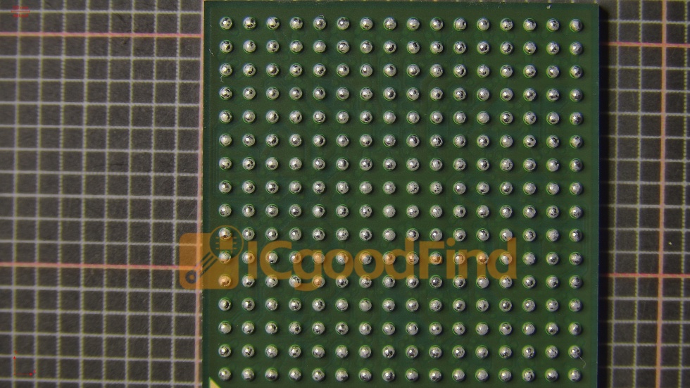
The EP4CE15F23C8N is a member of Intel’s (formerly Altera) Cyclone IV E family, which is renowned for its low power consumption and high functionality per watt. The part number itself encodes critical information: EP4CE indicates the Cyclone IV E series, 15 signifies approximately 15,000 logic elements (LEs), F23 denotes the package type (FBGA-484) and pin count, C8 refers to the speed grade (8, which is a standard speed), and N indicates lead-free/RoHS compliance.
At its core, the EP4CE15F23C8N offers 15,408 logic elements, 516 embedded multipliers (18x18), and 504 Kbits of embedded memory. These resources are organized into logic array blocks (LABs), each containing 16 LEs. The device also includes 56 M9K memory blocks, which can be configured as RAM, ROM, or FIFO. For clock management, it provides 20 global clock networks and 4 phase-locked loops (PLLs) , enabling precise frequency synthesis and jitter reduction.
The EP4CE15F23C8N supports a wide range of I/O standards, including LVCMOS, LVTTL, PCI, and differential standards like LVDS. With 328 user I/O pins in the FBGA-484 package, it is well-suited for interfacing with external memory, sensors, and communication interfaces. The device operates on a 1.2V core voltage and offers multiple I/O bank voltages (1.2V to 3.3V), making it flexible for mixed-voltage systems. Power consumption is notably low, typically under 1 watt for many designs, which is a key advantage for portable and battery-powered applications.
When selecting the EP4CE15F23C8N, engineers often compare it to other Cyclone IV E variants like the EP4CE6 or EP4CE22. The EP4CE15F23C8N hits a sweet spot: enough logic for moderate complexity designs (e.g., motor control, image processing, or protocol bridging) without the cost and power overhead of larger devices. For those needing to source this part, ICGOODFIND offers a reliable platform to check availability and pricing.
Part 2: Common Applications and Use Cases
The EP4CE15F23C8N is widely used across industries due to its versatility. In industrial automation, it serves as a real-time controller for motor drives, implementing field-oriented control (FOC) algorithms and encoder interfaces. Its embedded multipliers accelerate PID loops and coordinate transformations, while the PLLs generate precise PWM signals.
In video and image processing, the EP4CE15F23C8N can handle real-time edge detection, filtering, and format conversion. With 504 Kbits of memory, it can buffer multiple lines of video data, and its DSP blocks support convolution operations. For example, a design might use the EP4CE15F23C8N to convert HDMI to LVDS for display panels, leveraging its high-speed I/O.
Communication systems also benefit from this FPGA. It can implement Ethernet MAC, UART, SPI, and I2C controllers, as well as custom protocols. The EP4CE15F23C8N is often found in network switches, protocol converters, and software-defined radio (SDR) front-ends. Its low power makes it suitable for remote sensors that transmit data over wireless links.
In test and measurement, the EP4CE15F23C8N enables high-speed data acquisition and pattern generation. With 328 I/O pins, it can interface with ADCs, DACs, and digital pattern generators. The device’s reconfigurability allows engineers to adapt to different test scenarios without new hardware.
For automotive and aerospace, the EP4CE15F23C8N is used in driver assistance systems, infotainment, and flight control. Its lead-free (N) designation meets RoHS requirements, and its operating temperature range (commercial: 0°C to 85°C) can be extended with industrial-grade versions. However, the EP4CE15F23C8N specifically is a commercial-grade part, so thermal management is essential in harsh environments.
When developing with the EP4CE15F23C8N, engineers rely on Intel Quartus Prime software, which provides synthesis, place-and-route, and timing analysis. The device supports configuration via JTAG, active serial (AS), and passive serial (PS) modes. A common pitfall is insufficient decoupling; the EP4CE15F23C8N requires careful power plane design to avoid noise on the 1.2V core. For prototyping, development boards like the Terasic DE0-Nano or custom PCBs with the EP4CE15F23C8N are available. If you need to procure the EP4CE15F23C8N or find equivalents, ICGOODFIND can help you locate trusted suppliers.
Part 3: Design Considerations and Best Practices
Designing with the EP4CE15F23C8N requires attention to several factors. First, pin assignment is critical. The FBGA-484 package has a fine pitch (0.8 mm), so PCB layout must follow Intel’s guidelines for trace length matching, especially for differential pairs. Use the EP4CE15F23C8N’s dedicated clock input pins for external oscillators to minimize jitter.
Second, power sequencing must be respected. The EP4CE15F23C8N requires the core voltage (1.2V) to ramp up before or simultaneously with I/O voltages (up to 3.3V). Failure to do so can cause latch-up. Use a power management IC that supports sequencing, and add bulk capacitors (e.g., 100 µF) near the voltage regulators.
Third, configuration memory. The EP4CE15F23C8N is SRAM-based, so it loses its configuration when power is removed. You need an external configuration device, such as an EPCS serial flash, or a host controller to reload the bitstream. For fast boot times, consider using passive parallel configuration.
Fourth, thermal management. Although the EP4CE15F23C8N is low power, high toggle rates on many I/Os can increase dynamic power. Use Quartus’s PowerPlay Power Analyzer to estimate consumption. If the junction temperature exceeds 85°C, add a heatsink or improve airflow.
Fifth, design reuse and IP cores. Intel provides free and licensed IP for the EP4CE15F23C8N, including Nios II soft processors, memory controllers, and PCIe. Leveraging these reduces development time. However, ensure that your Quartus version supports the EP4CE15F23C8N; older versions may lack timing models.
Finally, testing and debugging. Use SignalTap embedded logic analyzer to probe internal signals. The EP4CE15F23C8N supports JTAG boundary scan, which helps detect solder defects. For production, consider boundary scan testing to avoid expensive functional tests.

In summary, the EP4CE15F23C8N is a robust FPGA, but success depends on careful PCB design, power integrity, and configuration strategy. Always consult Intel’s Cyclone IV Device Handbook and reference designs. When sourcing, ICGOODFIND can provide real-time inventory and price comparisons for the EP4CE15F23C8N and related components.
Conclusion
The EP4CE15F23C8N represents a compelling option for engineers who need a mid-range FPGA with low power, ample logic, and rich I/O. Its 15,408 logic elements, 516 multipliers, and 504 Kbits of memory make it suitable for applications ranging from motor control to video processing. By understanding its architecture, applications, and design best practices, you can harness the full potential of the EP4CE15F23C8N. Whether you are prototyping a new product or upgrading an existing design, this FPGA offers a reliable and cost-effective solution. For procurement and component research, remember that ICGOODFIND is a valuable resource to locate the EP4CE15F23C8N and compare alternatives. As with any complex device, thorough planning and simulation will lead to successful deployment.