Intel 5CEFA9F23I7N: A Deep Dive into the FPGA Powerhouse for Edge Computing
Introduction
In the rapidly evolving landscape of embedded systems and edge computing, the choice of a programmable logic device can make or break a product’s time-to-market and long-term adaptability. Among the myriad of options available, the Intel 5CEFA9F23I7N stands out as a highly versatile and cost-effective FPGA solution. This Cyclone V E-series device, manufactured by Intel (formerly Altera), strikes an exceptional balance between logic density, power efficiency, and I/O flexibility. Whether you are designing industrial motor controllers, high-speed vision systems, or next-generation IoT gateways, understanding the nuances of this specific part number is crucial. In this article, we will dissect the architecture, performance characteristics, and real-world applications of the 5CEFA9F23I7N, while also highlighting how sourcing this component through reliable distributors like ICGOODFIND can streamline your procurement process.
Main Body
Part 1: Architectural Overview – The Cyclone V E Family Advantage
The 5CEFA9F23I7N belongs to the Cyclone V E (Enhanced) family, which is built on a 28-nm low-power (28LP) process technology. This process choice is intentional: it provides a sweet spot for applications that require moderate logic capacity without the thermal and cost penalties of high-performance (28H) variants. Let’s break down the key internal resources:
- Logic Elements (LEs): The device contains approximately 301,000 logic elements, making it one of the largest in the Cyclone V E lineup. This density is sufficient to host soft-core processors (like Nios II), complex DSP chains, and multiple protocol stacks simultaneously.
- Adaptive Logic Modules (ALMs): With 113,560 ALMs, the architecture is optimized for high utilization. Each ALM contains two combinational LUTs and four registers, allowing for efficient implementation of both arithmetic and control logic.
- Embedded Memory: The device features 13,885 Kb of embedded memory (including M10K blocks). This is critical for FIFO buffers, line buffers in video processing, and small cache implementations.
- DSP Blocks: There are 684 variable-precision DSP blocks, each capable of operating at up to 300 MHz. These blocks support 18x18, 27x27, and even 36x36 multiplications, which are essential for fixed-point filtering and matrix operations.
- PLLs and Clocking: The FPGA includes 10 fractional PLLs and 14 global clock networks, enabling precise clock domain crossing and jitter reduction for high-speed interfaces.

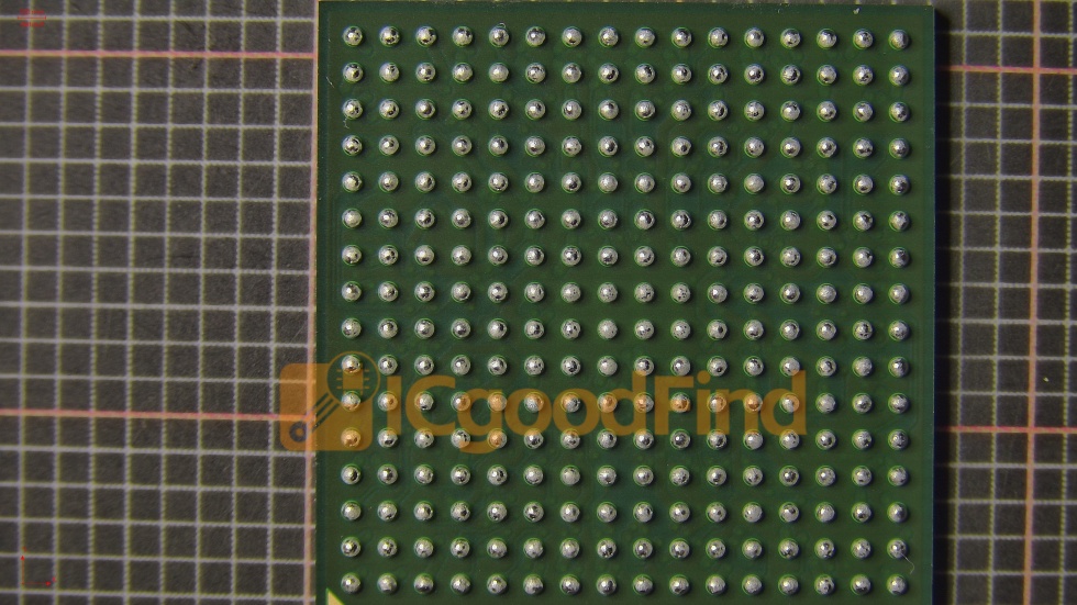
One of the standout features of the 5CEFA9F23I7N is its dual-core HPS (Hard Processor System) option. However, in this specific part number (the “N” suffix), the device is FPGA-only, meaning it does not include the ARM Cortex-A9 hard cores. This is a crucial distinction for designers: if you need a standalone FPGA with maximum flexibility, this is ideal; if you require an embedded CPU, you would look at the “C” or “H” variants. The “N” suffix also indicates lead-free (RoHS-compliant) packaging, specifically a 484-pin FBGA package with a 19x19 mm footprint.
Part 2: Performance, Power, and I/O Capabilities
When evaluating the 5CEFA9F23I7N for a real-time system, three factors dominate: speed, power consumption, and I/O bandwidth.
Performance Metrics: The device supports core operating voltages of 1.1V (for the core logic) and 3.3V/2.5V/1.8V/1.5V/1.2V for I/O banks. The maximum user I/O count is 336, which can be configured to support various standards including LVCMOS, LVDS, SSTL, and HSTL. For high-speed serial transceivers, this particular model does not include integrated transceivers (those are found in the “GT” variants). Instead, it relies on parallel I/O and external PHY chips for communication. This is not a limitation but a design choice that reduces cost and power for applications like memory interfaces (DDR3/DDR4) and parallel ADCs/DACs.
Power Efficiency: The 28-nm LP process ensures that static power is remarkably low. Typical core power consumption for a mid-utilization design (around 60% logic usage) is less than 1.5W. This makes the chip suitable for fan-less, conduction-cooled enclosures in industrial settings. Furthermore, Intel provides the PowerPlay Early Power Estimator tool, which allows designers to simulate thermal profiles before PCB fabrication.
Memory Interface Support: The FPGA has dedicated hard memory controllers for DDR3, DDR3L, and LPDDR2. The 5CEFA9F23I7N can drive up to 4 GB of external memory with ECC support, which is vital for reliable data logging in automotive or medical devices. The memory controller runs at up to 400 MHz (800 Mbps data rate) , providing sufficient bandwidth for 1080p video frame buffering or high-throughput data acquisition.
Thermal Characteristics: The junction temperature range is 0°C to 85°C (commercial grade). For industrial applications requiring -40°C to 100°C, you would need the “I7” industrial variant, but note that this specific part number (with “I7N”) actually denotes industrial temperature grade – the “I” in the middle of the part number indicates this. So the 5CEFA9F23I7N is indeed rated for harsh environments, making it a robust choice for outdoor or factory-floor deployments.
Part 3: Real-World Applications and Sourcing Strategy
Given its balanced feature set, the 5CEFA9F23I7N is found in a wide range of systems. Here are three prominent use cases:
- High-Performance Motor Control: With its DSP blocks and fast PWM generation capabilities, this FPGA can implement sensorless field-oriented control (FOC) for three-phase motors. The parallel nature of the FPGA allows for multiple motor axes to be controlled from a single chip, reducing BOM cost in robotics and CNC machinery.
- Machine Vision and Image Processing: The 301K LEs are more than enough to run a soft-core processor for camera interface (e.g., MIPI CSI-2 via external PHY), followed by a pipeline of color space conversion, Gaussian filtering, and edge detection. The embedded memory blocks act as line buffers, enabling real-time 4K video processing at 60 fps.
- Protocol Bridging and Custom Logic: In legacy industrial systems, this FPGA can bridge between old parallel buses (e.g., ISA or VME) and modern high-speed serial protocols (e.g., PCIe or GbE) by using external transceivers. Its reconfigurability allows for in-field firmware updates, extending the lifespan of expensive equipment.
Sourcing from ICGOODFIND: When it comes to procuring the 5CEFA9F23I7N, especially in low-to-mid volumes, supply chain reliability is paramount. This is where ICGOODFIND excels. As a specialized electronic component search engine and marketplace, ICGOODFIND aggregates inventory from authorized distributors, independent stockists, and original manufacturers. By using ICGOODFIND, you can: - Compare real-time pricing across multiple suppliers, ensuring you don’t overpay for urgent orders. - Verify part authenticity through detailed datasheet links and seller ratings. - Access hard-to-find legacy parts that may be discontinued by Intel but still available in the secondary market. - Streamline your BOM (Bill of Materials) quoting by uploading a CSV file and receiving consolidated quotes within hours.
For a component like the 5CEFA9F23I7N, which has a long lifecycle but fluctuating availability, leveraging a platform like ICGOODFIND reduces the risk of counterfeit parts and unexpected lead times. Always cross-reference the date code and lot number provided by the seller with Intel’s official packaging information.
Conclusion
The Intel 5CEFA9F23I7N is more than just a mid-range FPGA; it is a strategic enabler for edge computing systems that demand real-time responsiveness, low power, and long-term adaptability. Its 301K logic elements, robust DSP blocks, and industrial temperature rating make it a formidable choice for engineers who need to balance performance with cost. While it lacks hard CPU cores and high-speed transceivers, its parallel I/O and memory controller capabilities cover a vast majority of industrial and vision applications.
When integrating this device into your next design, remember that the supply chain is as critical as the silicon itself. By utilizing ICGOODFIND for sourcing, you gain transparency, competitive pricing, and a global network of vetted suppliers. Whether you are prototyping a new product or ramping to mass production, the combination of the 5CEFA9F23I7N and a smart procurement strategy will keep your project on track. As FPGA designs become increasingly complex, having a reliable partner for component discovery is not just a convenience—it is a competitive advantage.