TDA21520: The Next-Generation Power Stage IC for High-Efficiency Computing
Introduction
In the rapidly evolving landscape of power electronics, the demand for higher efficiency, greater power density, and superior thermal performance has never been more critical. As data centers, AI accelerators, and automotive systems push the limits of electrical consumption, designers are constantly seeking components that can deliver exceptional performance without compromising reliability. Enter the TDA21520 — a fully integrated power stage solution from Infineon that is redefining how engineers approach voltage regulator design. This article explores the architecture, key benefits, and real-world applications of the TDA21520, while also highlighting how sourcing this component through ICGOODFIND ensures authenticity, availability, and competitive pricing for your next project.
Main Body

Part 1: Architecture and Key Features of the TDA21520
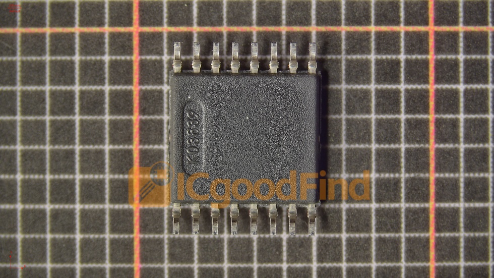
The TDA21520 is a dual-channel, 25 A continuous output current power stage IC designed for multi-phase buck converters. It integrates the high-side and low-side MOSFETs, gate drivers, and current-sense amplifier into a single compact package (5 mm x 5 mm PQFN). This integration eliminates the need for external driver components, reducing board space by up to 40% compared to discrete solutions.
One of the standout features of the TDA21520 is its adaptive dead-time control. This proprietary algorithm dynamically adjusts the switching timing between the high-side and low-side FETs based on load current and input voltage. The result is a significant reduction in body-diode conduction losses, which directly improves overall efficiency — especially at light loads where switching losses dominate. In typical 12 V to 1.8 V conversion scenarios, the TDA21520 achieves peak efficiency exceeding 94% , a figure that was previously only possible with expensive GaN or SiC devices.
Another critical architectural highlight is the integrated current-sense amplifier with ±3% accuracy. Unlike external sense resistors that introduce parasitic inductance and power loss, the TDA21520 uses a proprietary inductor DCR sensing method. This allows the controller to precisely monitor phase current without additional components, enabling accurate load-line regulation and adaptive voltage scaling (AVS) . For CPU and GPU power delivery, this translates into faster transient response — the IC can handle load steps of 50 A/µs with minimal voltage droop, ensuring stable operation under burst workloads.
Furthermore, the TDA21520 supports PWM frequency from 300 kHz to 2 MHz, giving designers flexibility to optimize for efficiency (lower frequency) or size (higher frequency). The device also features thermal flag output and over-temperature protection, which shuts down the driver if the junction temperature exceeds 150°C. This robust protection suite makes it suitable for harsh automotive and industrial environments where thermal cycling is a constant challenge.
Part 2: Performance Advantages and Comparison with Competing Solutions
When compared to earlier generation power stages like the TDA21470 or competing parts from MPS (MP86956) and Renesas (ISL99390), the TDA21520 offers clear performance leadership in three key areas: switching loss reduction, thermal impedance, and fault reporting.
First, switching loss reduction. The TDA21520 uses Infineon’s thin-film MOSFET technology with ultra-low gate charge (Qg = 8 nC typical). Combined with the adaptive dead-time control, this reduces the crossover loss during switching transitions by up to 30% compared to fixed dead-time designs. In a 6-phase VR design for a 400 W GPU, this translates to saving 4-5 W of power that would otherwise be dissipated as heat. Over a year of continuous operation, this saves approximately 40 kWh per server — a meaningful contribution to data center sustainability goals.
Second, thermal impedance. The package features an exposed pad with a low thermal resistance (θJC = 1.2 °C/W) . This is 20% lower than the industry average for similar form factors. When mounted on a standard 4-layer PCB with thermal vias, the TDA21520 can dissipate up to 3.5 W per phase without requiring active cooling. This allows designers to push output current to 25 A per phase at 85°C ambient, whereas competing parts typically derate to 20 A under the same conditions. For high-density designs like 48 V to 1 V direct conversion, this thermal headroom is invaluable.
Third, fault reporting and telemetry. The TDA21520 includes a PMBus-compatible SMBus interface that reports real-time phase current, temperature, and fault status. This digital telemetry enables predictive maintenance in server farms — the system can proactively reduce clock speed if a phase is running hotter than its siblings, preventing thermal runaway. Competing analog-only solutions lack this granularity, forcing designers to rely on external sense circuits that add cost and complexity.
It is also worth noting that the TDA21520 is pin-to-pin compatible with the TDA21570 (35 A version) and TDA21590 (50 A version). This scalability allows a single PCB layout to support multiple power tiers, reducing design risk and inventory costs. When sourcing these variants, ICGOODFIND provides a unified platform to compare stock levels across authorized distributors, ensuring you get the exact grade you need without long lead times.
Part 3: Application Scenarios and Design Considerations
The TDA21520 is optimized for three primary application domains: high-performance computing (HPC), automotive ADAS, and telecom infrastructure.
In HPC and AI accelerators, the TDA21520 is used in multi-phase VRM designs for CPUs (e.g., Intel Sapphire Rapids) and GPUs (e.g., NVIDIA H100). A typical 16-phase design can deliver up to 400 A continuous current at 1.0 V core voltage. The key design consideration here is loop stability — because the TDA21520 has very low output impedance, the controller must use a type-III compensator with a crossover frequency of 100-150 kHz to avoid subharmonic oscillation. Infineon provides reference designs and simulation models (SIMetrix) to accelerate this process. Additionally, the spread-spectrum PWM feature (up to ±15% dithering) helps reduce EMI, which is critical for passing FCC Class B radiated emission tests in dense server racks.
In automotive ADAS, the TDA21520 is used for sensor fusion processors (e.g., Mobileye EyeQ5) that require tight voltage regulation (±1%) under load transients caused by camera and LiDAR data bursts. The IC’s AEC-Q100 Grade 1 qualification (-40°C to +125°C) ensures reliable operation under extreme under-hood temperatures. Designers must pay attention to input voltage range — the TDA21520 operates from 4.5 V to 16 V, which covers 12 V battery systems but not 48 V mild-hybrid architectures. For those, Infineon offers the TDA21570-A1 with extended voltage rating. When sourcing automotive-grade parts, ICGOODFIND verifies the AEC-Q100 certificate and lot traceability for each reel, eliminating the risk of counterfeit or re-marked components.
In telecom and 5G base stations, the TDA21520 is used for FPGA and ASIC power in remote radio units (RRUs). The key challenge here is high ambient temperature (often >70°C) inside sealed outdoor enclosures. The TDA21520’s low thermal resistance allows it to operate at 20 A per phase with only a heatsink attached to the PCB’s bottom side. For optimal thermal performance, designers should use 4-layer PCBs with 2 oz copper on all layers and place thermal vias directly under the exposed pad. Additionally, the power-good output can be tied to a system watchdog to trigger a safe shutdown if the output voltage falls outside the ±5% window — a crucial safety feature for remote installations where physical access is limited.
One common pitfall when using the TDA21520 is incorrect bootstrap capacitor selection. The bootstrap capacitor (CBOOT) must be at least 100 nF with a 25 V rating, placed within 5 mm of the BOOT pin. Using a smaller capacitor will cause high-side gate drive undervoltage, leading to increased RDS(on) and potential thermal shutdown. ICGOODFIND offers a design support portal where engineers can download verified BOMs and layout guidelines for the TDA21520, reducing the risk of first-pass hardware failures.
Conclusion

The TDA21520 represents a significant leap forward in integrated power stage technology, combining adaptive dead-time control, ±3% current sensing, and robust digital telemetry in a compact, thermally efficient package. Whether you are designing a 400 W GPU VRM, an automotive ADAS processor, or a 5G RRU power supply, this IC delivers the efficiency and reliability required to meet stringent performance targets. Its scalability across the TDA215xx family further simplifies platform reuse, while the AEC-Q100 qualification ensures automotive-grade robustness.
To fully leverage the TDA21520’s capabilities, sourcing from a trusted distributor is paramount. ICGOODFIND provides real-time inventory visibility across global suppliers, competitive pricing, and full traceability documentation — ensuring you receive genuine Infineon parts with factory-sealed packaging. With ICGOODFIND, you can also access application notes and reference designs that cut development time by weeks. As power densities continue to rise, the TDA21520 — paired with a reliable supply chain — is your strategic advantage in building the next generation of high-efficiency systems.