The Rise of the Smallest MCU: Powering the Next Generation of Smart Devices
Introduction
In the relentless march of technological miniaturization, a quiet revolution is unfolding at the heart of embedded systems. The quest for the Smallest MCU (Microcontroller Unit) is not merely an engineering curiosity; it is a fundamental driver behind the proliferation of the Internet of Things (IoT), wearable technology, and disposable medical devices. These minuscule silicon brains, often smaller than a grain of rice, encapsulate a processor core, memory, and programmable input/output peripherals, enabling intelligence to be embedded into virtually any object. As products demand lower power consumption, smaller form factors, and lower costs, the competition to deliver the most feature-dense, ultra-compact microcontroller has intensified. This article explores the world of the smallest MCUs, examining their architecture, groundbreaking applications, and the critical design considerations they entail. For engineers and procurement specialists navigating this complex landscape, platforms like ICGOODFIND provide invaluable resources for comparing specifications, availability, and sourcing these critical components efficiently.
Main Body
Part 1: Defining “Small” – Architecture and Packaging Breakthroughs
The term “smallest” in MCUs is multidimensional, referring to package size, power footprint, and the minimal system component count. Achieving extreme miniaturization hinges on two key areas: advanced semiconductor packaging and architectural ingenuity.
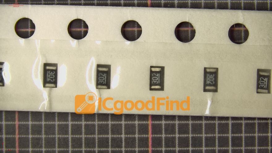
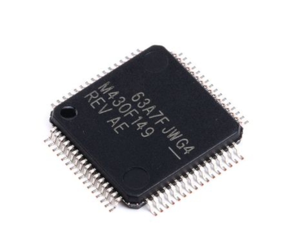
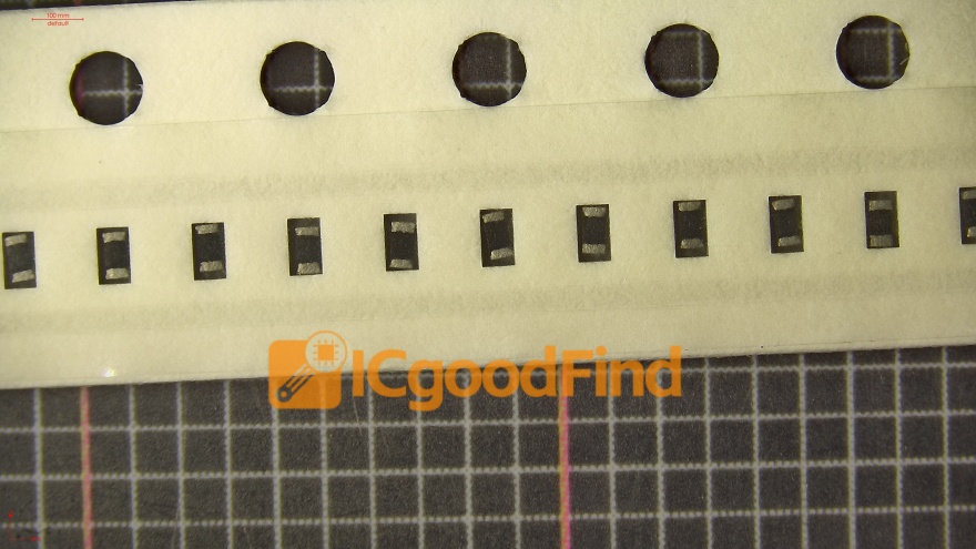
First, packaging technology has evolved dramatically. Traditional packages like QFP and SOIC have given way to Wafer-Level Chip-Scale Packages (WLCSP). In WLCSP, the bare die is packaged and connected directly to the circuit board, with the final package being nearly identical in size to the silicon die itself. This results in packages measuring just 1.6 x 1.6 mm or even smaller. Companies like STMicroelectronics, NXP Semiconductors, and Texas Instruments are pushing these boundaries, offering MCUs in packages with ball pitches as fine as 0.3mm.
Second, architectural integration is paramount. The goal is to maximize functionality per square millimeter. Modern ultra-compact MCUs integrate not just a CPU core (often Arm Cortex-M0+ or proprietary ultra-low-power cores) and flash memory but also essential analog and digital peripherals. Key integrated components now routinely include: * Ultra-Low-Power Analog Comparators and ADCs for sensor interfacing. * On-chip DC-DC Converters to regulate voltage efficiently from a single battery. * Radio Transceivers (in System-on-Chip designs) for Bluetooth Low Energy (BLE) or proprietary wireless protocols. * Capacitive Touch Sensing interfaces.
This high level of integration reduces the need for external components, shrinking the total PCB footprint and simplifying design—a critical factor for disposable or massively deployed devices.
Part 2: Revolutionizing Applications – Where Tiny Brains Make a Big Impact
The advent of sub-2mm MCUs has unlocked entirely new product categories and enhanced existing ones by making embedded intelligence practically invisible and inexpensive.
1. Consumer Electronics and Wearables: This is perhaps the most visible domain. The smallest MCUs are the enablers of true wireless earbuds, hearing aids with advanced features, smart rings for fitness tracking, and disposable electronic patches. Their minimal power draw allows for extended operation in devices where battery space is severely constrained. For instance, a smart label on retail clothing can now contain an MCU-powered NFC or RFID tag for inventory management and anti-counterfeiting.
2. Medical and Healthcare Disposables: This field presents one of the most compelling cases. Single-use medical devices, such as smart pill bottles that track adherence, connected drug delivery pens (e.g., for insulin), and diagnostic patches that monitor vital signs before being discarded, rely entirely on MCUs that are cheap enough to be disposable yet capable enough to collect and transmit data reliably.
3. Industrial IoT and Asset Tracking: Deploying thousands of sensors across a factory floor or a supply chain requires each node to be low-cost and unobtrusive. Miniature MCUs power wireless sensor nodes that monitor temperature, humidity, vibration, or location. Their small size allows them to be embedded directly into machinery parts, product packaging, or even tools themselves.
4. Edge AI and Machine Learning: The frontier is now about embedding not just control logic but simple inference models into these tiny devices. With core architectures evolving and leveraging hardware accelerators for specific tasks like keyword spotting or anomaly detection, the smallest MCUs are beginning to process data locally at the extreme edge, reducing latency and cloud dependency.
Part 3: Navigating the Design Challenges
Designing with the world’s smallest MCUs is not without significant hurdles. Engineers must balance extreme constraints across multiple fronts.
Power Management is Paramount: With batteries sometimes as small as coin cells or even using energy harvesting techniques, every microampere counts. Developers must master deep sleep modes with nanoampere-level current draw, rapid wake-up cycles, and intelligent peripheral scheduling to maximize operational life. The MCU’s integrated power management features become as important as its processing speed.
PCB Design Complexity Increases Exponentially: Working with WLCSP packages with microscopic ball pitches demands high-precision manufacturing capabilities. Design rules become extremely stringent: layer count may increase to route traces from under the package, impedance control is critical for any integrated radios, and thermal management must be considered even for low-power chips due to their minuscule thermal mass.
Debugging and Development Hurdles: The physical lack of pins makes traditional in-circuit debugging (ICT) and programming difficult or impossible after assembly. Developers rely heavily on Software Development Kits (SDKs) with robust simulation tools and pre-programmed modules before final production programming via bed-of-nails test fixtures or wireless methods.
In this complex ecosystem, finding the right component that balances size, features, power, cost, and long-term availability is a daunting task. This is where specialized component search and sourcing platforms prove indispensable. A platform like ICGOODFIND streamlines this process by allowing engineers to filter MCUs by critical parameters such as package dimensions, core type, peripheral mix, and power profiles from a vast cross-section of global suppliers, significantly accelerating the prototyping and procurement phases.
Conclusion
The pursuit of the Smallest MCU represents a foundational trend in electronics, moving computing from boxes to everyday items—and ultimately into virtually invisible form factors. These technological marvels are far more than just shrunk-down versions of their larger counterparts; they are purpose-built engines of innovation for a connected, sensor-rich world. From transforming healthcare with intelligent disposables to enabling ubiquitous sensing in industrial settings, their impact is profound. While designing with them presents unique challenges in power optimization, PCB layout, and development workflows, the tools and resources available to engineers—including comprehensive component databases—continue to evolve in tandem. As semiconductor technology advances further with 3D stacking and new materials like FD-SOI (Fully Depleted Silicon-On-Insulator), we can expect these microscopic controllers to become even more powerful and efficient. The future belongs not just to faster processors but to smarter ones that can be placed anywhere—and the smallest MCUs are leading that charge.