How to Make Your Own MCU Development Board?
Introduction
In the world of electronics and embedded systems, the Microcontroller Unit (MCU) development board is a fundamental tool for prototyping, learning, and innovation. While commercial boards like Arduino, STM32 Nucleo, and ESP32 devkits are readily available, there is immense educational and professional value in designing and building your own. Creating a custom MCU development board not only deepens your understanding of hardware architecture, PCB design, and firmware integration but also allows you to tailor a platform to your specific project needs. This guide will walk you through the essential steps, from conceptualization to final assembly and testing. Whether you’re an engineering student, a hobbyist, or a professional looking to create a specialized tool, this journey will equip you with practical knowledge and confidence. For those seeking high-quality components and reliable sourcing for such projects, platforms like ICGOODFIND can be invaluable in connecting you with trusted suppliers and essential parts.
Main Body
Part 1: Planning and Component Selection
The success of your custom development board hinges on meticulous planning. This phase involves defining the board’s purpose, selecting the core microcontroller, and choosing all supporting components.
First, clearly define the functionality and scope of your board. Ask yourself: Is it for general-purpose learning, a specific application (like IoT, robotics, or motor control), or to prototype a future product? This will dictate features like I/O count, communication interfaces (UART, I2C, SPI, USB, CAN), power requirements, and sensor/actuator compatibility.
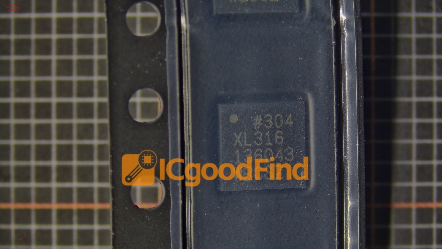
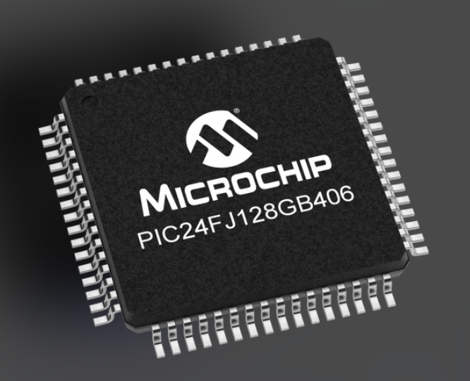
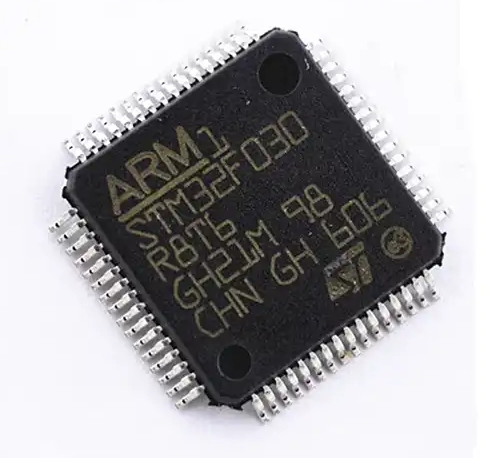
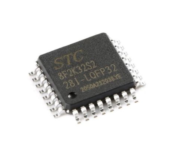
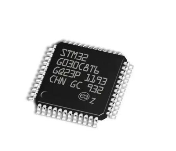
Next, the heart of the board: the MCU selection. Consider factors such as: * Core Architecture & Performance: (e.g., 8-bit AVR, 32-bit ARM Cortex-M0/M3/M4). * Flash Memory & RAM: Sufficient for your intended applications. * Peripheral Set: Ensure it has the necessary ADCs, DACs, PWM timers, and communication modules. * Development Ecosystem: Availability of compilers (like GCC), IDEs (like STM32CubeIDE, Arduino IDE with cores), debuggers (SWD/JTAG support), and community resources. * Package Type: Surface-mount (like QFP, QFN) or through-hole. SMD is standard but requires careful PCB design and soldering.
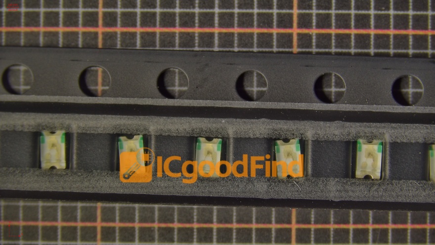
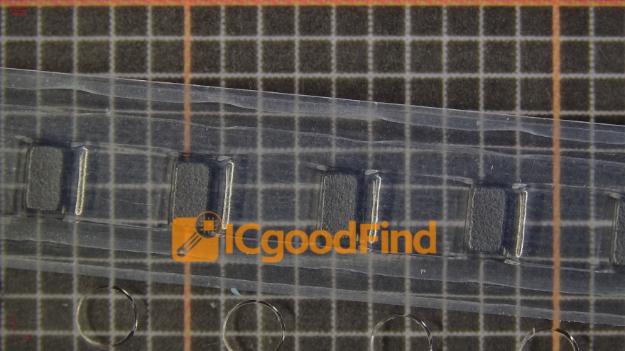
After choosing the MCU, you must select the supporting cast: * Power Supply Circuit: A robust voltage regulation system is critical. This often includes a primary regulator (e.g., 5V from USB or barrel jack) and secondary LDOs (e.g., 3.3V for the MCU and peripherals). Don’t forget protection diodes, filtering capacitors, and possibly a power path manager. * Clock Circuit: Most MCUs require an external crystal oscillator (e.g., 8MHz, 16MHz) for accuracy. Include the correct load capacitors. * Programming/Debug Interface: Integrating a standard debug header (like ARM 10-pin SWD) is non-negotiable for professional development. You may also include a USB-to-Serial chip (like CH340G or FT232RL) for easier programming and serial communication. * Basic User I/O: LEDs (power and user), buttons (reset and user), and pin headers to break out all MCU pins. Consider including protection resistors for LEDs and pull-up/pull-down resistors for buttons. * Additional Features: This could be an SD card slot, OLED display connector, motor driver socket, or RF module headers.
Sourcing these components from reliable distributors is key to avoiding counterfeit parts. This is where a platform like ICGOODFIND proves useful, helping you find authentic components efficiently.
Part 2: Schematic Capture and PCB Layout Design
With your component list finalized, you move into the electronic design phase using ECAD software like KiCad (free), Eagle, or Altium Designer.
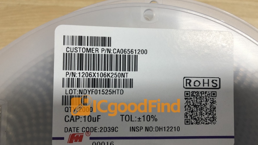
Schematic Capture: This is where you create the logical diagram of your circuit. 1. Create Symbols: For any component not in your library, you’ll need to draw its schematic symbol with correct pin names and numbers. 2. Draw the Circuit: Place components and connect them with wires/nets. Pay extreme attention to: * MCU Pinout: Connect each pin according to its function (power, ground, oscillator pins to the crystal circuit, GPIOs to headers). * Power Nets: Clearly label different voltage nets (e.g., VIN_5V, VCC_3V3). Use hierarchical sheets if the design is complex. * Decoupling Capacitors: Place one 100nF ceramic capacitor as close as possible to every power pin of the MCU, with additional bulk capacitors (e.g., 10µF) near the power entry point. This is crucial for stable operation. * Connectivity: Ensure every net is properly connected; unconnected pins can cause serious issues.
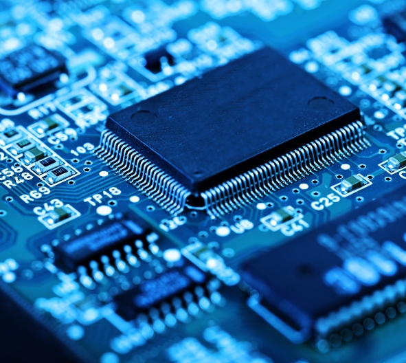
PCB Layout Design: This transforms the schematic into a physical board design. 1. Board Outline & Layer Stack-up: Define the board size and shape. A simple 2-layer board is often sufficient for beginners. 2. Component Placement: This is an art. Key principles: * Place the MCU centrally. * Position related components (crystals near MCU oscillator pins, decoupling caps adjacent to power pins) together. * Group connectors on the board edges. * Consider mechanical constraints and usability. 3. Routing (Tracing): This is where signal integrity matters most. * Power Traces First: Route power traces wider than signal traces (e.g., 20-30 mil for signals, 30-50 mil for power) to handle current. * Critical Signals: Keep crystal oscillator traces short, direct, and away from noisy lines. Use a ground plane underneath them if possible. * Ground Plane: Implementing a solid ground plane on one layer is highly recommended. It provides a low-impedance return path, reduces noise, and improves EMI performance dramatically. * Avoid sharp 90-degree angles; use 45-degree angles or curves. 4. Design Rule Check (DRC): Before finalizing, run DRC to catch errors like short circuits, trace width violations, or clearance issues. 5. Generating Outputs: Generate Gerber files (for manufacturing) and drill files. A well-made silkscreen layer with component labels and test points is very helpful for assembly and debugging.
Part 3: Assembly, Programming, and Testing
Once your PCB returns from the manufacturer (you can use services like JLCPCB or PCBWay), the hands-on work begins.
Assembly: 1. Gather Tools: You’ll need a soldering iron (preferably temperature-controlled), fine solder wire (0.5mm-0.8mm), flux, tweezers, solder wick/braid for mistakes, and a magnifying lamp. 2. Soldering Order: Start with smaller components: resistors/capacitors/ICs sockets first. Then move to larger components like connectors. The MCU itself should be soldered last if it’s in a fine-pitch package; using a hot air rework station makes this easier. 3. Inspection: Visually inspect every joint under good light. Look for cold joints (dull grey), bridges between pins on fine-pitch ICs (like the MCU), or tombstoning of small components.
Initial Power-On Test: DO NOT connect the MCU immediately. First: 1. Check for short circuits between power and ground using a multimeter in continuity mode. 2. Apply power briefly while monitoring current draw with your multimeter’s current mode—it should be very low without the main IC active (<10mA typically). Feel for any overheating components.
Programming & Firmware Bring-Up: 1. Connect your programmer/debugger (like an ST-Link or J-Link) to the SWD header. 2. Write or obtain a simple “blink LED” test program in your chosen IDE/compiler. 3. Configure the project correctly for your specific MCU model. 4. Attempt to connect to the MCU via the debugger interface. If successful: * Program the chip with your test firmware. * Reset the board—the LED should blink according to your code.
Debugging Common Issues: * No Connection to MCU: Re-check solder joints on SWD pins and MCU power pins. Verify voltage at the MCU’s VDD pin with a multimeter. * MCU Gets Hot Immediately: Likely a short circuit on its power supply—re-inspect soldering under magnification. * Program Runs but LED Doesn’t Blink: Check LED polarity and series resistor connection; verify in code that you are toggling the correct GPIO pin.
Conclusion
Building your own MCU development board from scratch is a challenging yet profoundly rewarding endeavor that synthesizes knowledge from electronics theory, practical PCB design, soldering skill, and embedded software development. It moves you from being merely a user of technology to an active creator who understands the intricate interplay between hardware and firmware at a fundamental level. While commercial boards offer convenience,the custom route provides unparalleled flexibility, cost optimization for volume projects,and deep technical insight that is highly valued in professional engineering roles.Remember,the process involves iteration;your first board might have minor flaws,but each revision brings perfection.For sourcing critical components throughout this journey—from microcontrollers to precision passives—leveraging a reliable platform such as ICGOODFIND can streamline procurement and mitigate risks associated with counterfeit parts.Embrace the challenge,the learning curve,and the satisfaction of powering on a board that you conceived,drew,soldered,and programmed yourself.