

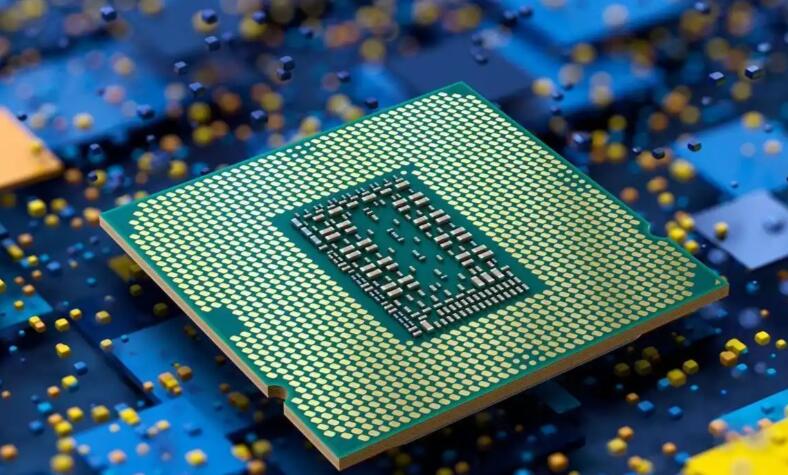
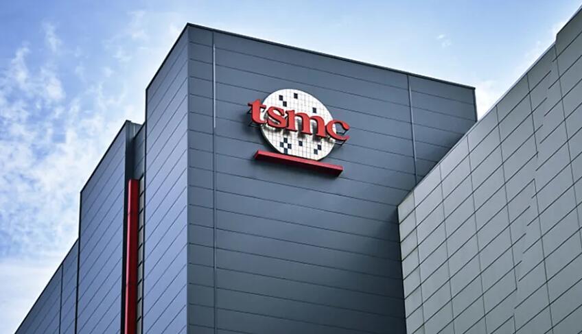


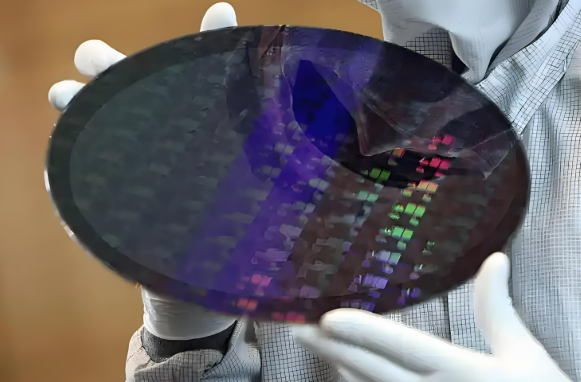
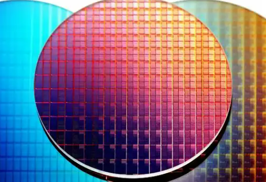
TSMC has made significant progress in 1.4nm technology, with its A14 node reportedly meeting yield targets ahead of schedule. Compared to the upcoming 2nm (N2) process, A14 delivers substantial improvements in performance and efficiency.
Official data indicates that the A14 process offers 15% higher speed at the same power, or 30% lower power consumption at matched speed, while increasing logic density by 20%. These gains are enabled by second-generation GAAFET nanosheet transistors and the new NanoFlex Pro standard cell architecture, which enhances both performance and design flexibility.
Unlike the A16 and certain 2nm variants that rely on super power rails (SPR) and backside power delivery networks (BSPDN), A14 adopts a BSPDN-free architecture. This makes it more suitable for client devices and edge computing applications that require a balance of performance and power efficiency. The node is expected to enter mass production in 2028, with Apple, AMD, and NVIDIA seen as key potential customers.
Competitor Intel is accelerating its efforts, having secured ASML’s entire 2024 output of high-NA EUV lithography tools—each costing approximately $370 million—to support its 14A process. Intel’s 14A node will use a second-generation PowerVia backside power delivery and RibbonFET 2 gate-all-around technology, targeting production in 2027.
While TSMC’s A14 utilizes conventional EUV technology to control costs, Intel is betting on high-NA EUV for a technological edge. The competition between TSMC’s A14 and Intel’s 14A is expected to intensify in the 2027–2028 timeframe.
ICgoodFind : The race between leading foundries will accelerate the adoption of advanced nodes, powering future innovations in AI and high-performance electronics.


