
The Evolution and Future of DRAM Process Technology
Introduction
Dynamic Random-Access Memory (DRAM) is the ubiquitous, high-speed working memory at the heart of virtually every modern computing device, from smartphones and laptops to data center servers. Its primary function is to temporarily store data that the processor needs immediate and rapid access to, acting as a critical bridge between the blazing-fast CPU and the slower, persistent storage. The performance, capacity, and power efficiency of DRAM are not merely products of design but are fundamentally dictated by its manufacturing process technology. The DRAM process refers to the intricate set of semiconductor fabrication techniques and lithography scales used to create the memory cells, capacitors, and transistors on a silicon wafer. This relentless scaling and innovation in process technology have been the primary engine driving Moore’s Law in the memory sector, enabling exponential growth in density and performance over decades. As we push against physical and economic limits, understanding the current state and future trajectory of DRAM process advancement is crucial for anticipating the next leaps in computing capability.
Main Body
Part 1: The Foundation - Core Concepts and Scaling Challenges
At its core, a DRAM cell is astonishingly simple: it consists of one transistor and one capacitor. The transistor acts as a gatekeeper, controlling access to the capacitor, which stores a single bit of data as an electrical charge (a “1” or “0”). The DRAM process is fundamentally about miniaturizing these billions of cells to pack more memory into a smaller area, thereby increasing density and reducing cost per bit.
The most critical metric in this journey has been the process node, historically measured in nanometers (nm). Moving from nodes like 30nm to 20nm, 1x-nm, 1y-nm, and now into the 1z-nm and sub-10nm era represents successive generations of scaling. Each shrink presents monumental challenges:
- Capacitor Scaling: As cells shrink, the capacitor’s physical size decreases, reducing its charge storage capacity. This makes the stored signal more susceptible to noise and leakage, potentially leading to data corruption. Innovations in capacitor structure—such as deeper cylinder shapes and high-k dielectrics—have been paramount to maintaining sufficient charge in a vanishingly small space.
- Transistor Performance: The access transistor must switch quickly and leak minimal current when off. Process advancements involve new transistor architectures and materials to meet these demands at smaller scales.
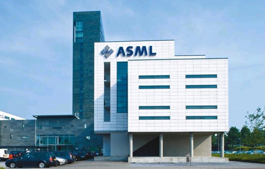
- Lithography Limits: Patterning features smaller than the wavelength of light requires increasingly complex and expensive techniques. The adoption of Extreme Ultraviolet (EUV) lithography has become a game-changer for advanced DRAM processes, allowing for cleaner, more precise patterning at nodes beyond 1y-nm, reducing multi-patterning steps and improving yield.
- Interconnect Complexity: Wiring up billions of cells with multiple layers of metal interconnects becomes exponentially more difficult. RC delay (resistance-capacitance delay) and parasitic capacitance can hamper speed and power efficiency.
These intertwined challenges mean that DRAM process scaling is no longer just about geometric shrinkage; it is a holistic co-optimization of materials, device structures, and integration schemes.
Part 2: Cutting-Edge Innovations in Modern DRAM Processes
To overcome these barriers, the industry’s leaders—Samsung, SK Hynix, and Micron—are deploying a suite of advanced technologies in their latest-generation processes (often referred to as 1β, 1γ, and beyond).
- EUV Lithography Dominance: While initially adopted cautiously, EUV is now critical for defining the most challenging layers in leading-edge DRAM. It simplifies the manufacturing process for critical cell patterns, leading to better performance uniformity, higher density, and improved production efficiency. The strategic implementation of EUV layers is a key differentiator in current-generation DRAM process technology.
- Novel Cell Architectures: Beyond simple planar scaling, new cell designs are emerging. For instance, buried wordline (BWL) architectures have become standard, where the wordline is embedded within the silicon substrate, reducing cell size and interference. Further innovations like multi-deck or 3D-stacked DRAM cells are being researched as potential paths forward when planar scaling becomes untenable.
- Advanced Materials Engineering: The search for better materials is relentless. This includes:
- High-k materials for capacitors to enhance charge storage.
- New channel materials for transistors to improve drive current.
- Low-resistance metals (like ruthenium) for wordlines and bitlines to reduce latency and power consumption.
- Hybrid Bonding & 3D Integration: While DRAM itself remains largely 2D, 3D integration techniques are becoming vital. Hybrid bonding allows for the direct, dense vertical stacking of multiple DRAM dies, enabling products like High Bandwidth Memory (HBM). HBM stacks multiple DRAM chips vertically with a logic base die using through-silicon vias (TSVs), achieving extraordinary bandwidth essential for AI and high-performance computing. This represents a shift from “scaling down” to “stacking up” for performance gains.
For professionals navigating this complex supply chain to source these advanced components or related electronic parts, platforms like ICGOODFIND can be an invaluable resource. It connects buyers with a global network of suppliers, helping to locate specific memory chips or ICs built on these cutting-edge processes.
Part 3: The Future Trajectory - Beyond Conventional Scaling
The path forward for DRAM process technology will be defined by both evolutionary improvements and potential revolutionary shifts.
- Continued Node Evolution: The march of EUV-based scaling will continue into the sub-10nm realm (e.g., 1δ-node). Expect increased use of EUV layers for more patterning steps, further driving down costs and complexity associated with multi-patterning.
- The Rise of Specialized DRAM: The “one-size-fits-all” approach is fading. Process technologies will be increasingly tailored for specific applications:
- LPDRAM: Ultra-low-power processes for IoT and mobile devices.
- HBM Processes: Optimized for high-speed interconnects, thermal performance, and stacking yield.
- High-Density Server DRAM: Focused on reliability, stability, and maximum capacity.
- Integration with Logic (CIM & Near-Memory Computing): One of the most promising frontiers is breaking down the “memory wall”—the bottleneck between processor and memory. Process technologies that enable Compute-In-Memory (CIM) architectures, where processing elements are integrated directly into the DRAM array or periphery using compatible logic processes, could dramatically reduce data movement energy and latency for AI workloads.
- Fundamentally New Architectures: In the longer term, if conventional 1T-1C cell scaling truly hits a wall, more radical changes may be needed. This could include the commercial exploration of alternative capacitor-less DRAM concepts (like Gain-Cell or Z-RAM) or even the integration of entirely new memory technologies that are easier to scale.
Conclusion
The journey of DRAM process technology is a testament to semiconductor innovation’s relentless pace. It has evolved from straightforward geometric scaling into a sophisticated discipline that masterfully combines cutting-edge lithography like EUV, novel materials science, innovative 3D integration schemes such as hybrid bonding for HBM, and application-specific optimization. While physical challenges are intensifying, the industry’s roadmap indicates a clear path forward through continued miniaturization supported by EUV and a strategic shift toward vertical integration and specialization. The ultimate goal remains unchanged: to deliver faster, denser, more power-efficient, and cost-effective memory that fuels progress across every sector of technology. The future of computing—particularly in the age of AI—will be inextricably linked to the success of these ongoing advancements in DRAM manufacturing processes.