The Ultimate Guide to MCU Hardware Development: From Concept to Circuit
Introduction
In the ever-evolving landscape of electronics, Microcontroller Unit (MCU) Hardware Development stands as the foundational pillar for countless innovations. From smart home devices and wearable technology to advanced industrial automation and the Internet of Things (IoT), MCUs serve as the intelligent “brain” embedded within hardware systems. This development process is a sophisticated interplay of electrical engineering, software integration, and meticulous design strategy, transforming abstract ideas into tangible, functional devices. For engineers and product developers, mastering this discipline is not just a technical skill but a critical competitive advantage in bringing efficient, reliable, and cost-effective products to market. This guide delves deep into the core principles, stages, and best practices that define successful MCU hardware development.
Main Body
Part 1: Foundational Stages and Strategic Planning
The journey of MCU hardware development begins long before the first schematic is drawn. This initial phase is arguably the most critical, as it sets the trajectory for the entire project.
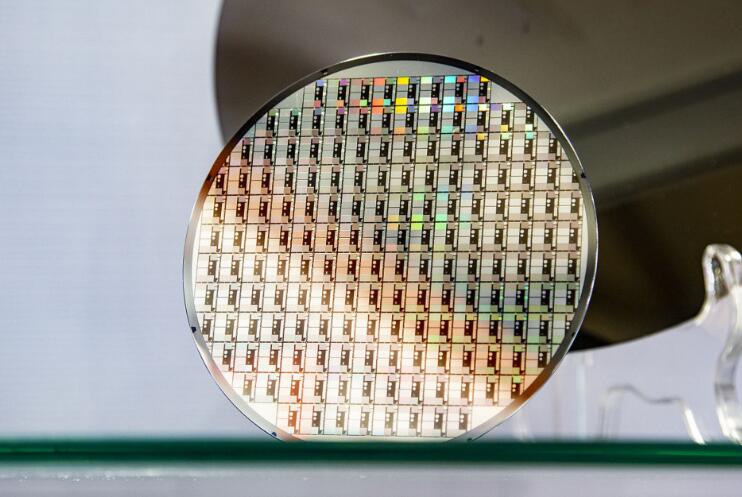
- Requirements Analysis and MCU Selection: The process starts with a clear definition of the product’s functional and non-functional requirements. Key questions must be answered: What is the core task? What peripherals are needed (e.g., ADC, DAC, PWM, communication interfaces like UART, SPI, I2C)? What are the power consumption constraints? What is the target cost? The answers directly inform the critical choice of the MCU. Engineers must evaluate architectures (e.g., ARM Cortex-M, AVR, PIC, RISC-V), clock speed, flash/RAM memory size, number of GPIO pins, and integrated peripherals. Selecting an MCU with excessive capabilities inflates cost, while an underpowered one can doom the project.
- Schematic Capture and Circuit Design: With the MCU selected, the schematic design phase commences. This involves creating a logical diagram of all electrical connections. Power supply design is paramount, requiring careful regulation, filtering, and decoupling to ensure a stable voltage rail for the MCU and other components. The reset circuit, clock generation (whether using internal or external crystals), and programming/debugging interface (like SWD or JTAG) must be meticulously designed. Furthermore, the schematic must include all necessary support circuitry for sensors, actuators, and communication modules (Wi-Fi, Bluetooth, LoRa).
- Component Sourcing and Design for Manufacturing (DFM): Concurrently, component selection and sourcing are vital. Factors like availability (avoiding obsolete parts), cost, package type (through-hole vs. surface-mount), and temperature ratings are considered. Early engagement with Design for Manufacturing (DFM) principles ensures the board can be assembled reliably at scale. This includes component placement for automated pick-and-place machines, thermal management considerations, and test point accessibility.
Part 2: PCB Layout, Prototyping, and Validation
Once the schematic is finalized and components are selected, the focus shifts to the physical embodiment of the design: the Printed Circuit Board (PCB).
- PCB Layout - Where Art Meets Engineering: The PCB layout process translates the schematic into a physical board design. This stage has a profound impact on performance and reliability. Proper grounding strategies, such as using ground planes, are essential to minimize noise and electromagnetic interference (EMI). Signal integrity must be preserved by carefully routing high-speed traces, matching lengths for differential pairs, and avoiding crosstalk. Power traces need to be sufficiently wide to handle current loads without excessive heating. Component placement is a balancing act between logical grouping, thermal dissipation, and mechanical constraints within the product enclosure.
- Prototype Fabrication and Assembly: The designed PCB files (Gerber files) are sent to a manufacturer for fabrication. For initial prototypes, services offering quick-turn PCBs are invaluable. Upon receiving the bare boards, components are soldered onto them. This can be done in-house for simple boards or through professional assembly services. The result is a working prototype, or “bring-up” board, which represents the first physical version of the design.
- Hardware Validation and Testing: This phase involves rigorous testing to ensure the hardware functions as intended. Power-up tests check for short circuits or incorrect voltages. Using tools like oscilloscopes, logic analyzers, and multimeters, engineers verify signal integrity, clock stability, and communication bus activity. Basic firmware is often written to “blink an LED” or read a sensor, confirming that the MCU can be programmed and interacts correctly with peripherals. Systematic validation at this stage identifies design flaws before they become costly in mass production.
Part 3: Firmware Integration and System Optimization
Hardware does not operate in a vacuum; its potential is unlocked by software. This phase bridges the gap between silicon and a fully operational product.
- Developing the Hardware Abstraction Layer (HAL): Firmware development begins with creating or utilizing a Hardware Abstraction Layer. A HAL provides a set of driver functions that interface directly with the MCU’s registers for GPIO control, timer configuration, ADC readings, etc. This layer abstracts the low-level hardware complexities, making the application code more portable and readable. Whether using vendor-provided libraries (like STM32Cube or ESP-IDF) or writing custom drivers, a robust HAL is crucial.
- System Integration and Debugging: With basic drivers in place, application-specific logic is integrated. This is where functionalities converge—reading sensor data, processing it with algorithms, making decisions, controlling outputs, and communicating with other devices. Debugging becomes a central activity, utilizing integrated development environments (IDEs), in-circuit debuggers (like ST-Link or J-Link), and serial console outputs to trace code execution and identify issues in both hardware interaction and software logic.
- Performance Tuning and Power Optimization: The final step involves refining the system for optimal performance. This may include optimizing code for speed or memory footprint, implementing low-power sleep modes to extend battery life in portable devices, and enhancing system robustness against electrical noise or unexpected events. Tools like profilers and power analyzers are indispensable here. For teams seeking comprehensive resources to streamline this entire development lifecycle—from component selection to firmware libraries—platforms like ICGOODFIND can be instrumental in aggregating technical data sheets, application notes, supplier information, and community insights in one centralized location.
Conclusion
MCU hardware development is a multifaceted discipline that demands a holistic approach combining strategic planning, rigorous electronic design principles, practical PCB layout skills, and seamless firmware integration. Each stage—from initial MCU selection and schematic design through PCB layout prototyping to final system optimization—is interconnected; a oversight in one phase can lead to significant challenges downstream. Success hinges on meticulous attention to detail at every step: stable power delivery clean signal integrity intelligent component placement robust firmware architecture By mastering this end-to-end process engineers empower themselves to create innovative reliable embedded systems that form backbone of modern technology As projects grow in complexity leveraging specialized resources becomes key to efficient development ultimately accelerating time-to-market for next generation of smart connected devices.