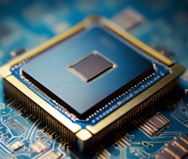
NVIDIA announced a major milestone: the first Blackwell architecture wafer has been produced at TSMC's Arizona facility in Phoenix, with CEO Jensen Huang and TSMC's operations VP Wang Yinglang signing the wafer to commemorate the event. This marks the start of mass production for NVIDIA's flagship AI chips on US soil.
Huang emphasized this as a historic achievement for US semiconductor manufacturing, calling it the first time the "most important chip" has been made domestically using TSMC's advanced technology. The Blackwell architecture delivers significant performance gains—11x faster inference for large language models, with 7x more compute power and 4x greater memory than its predecessor.
The production advance is a key step in TSMC's $65 billion US investment, supporting nodes like 2nm, 3nm, 4nm, and A16 for AI and high-performance computing. NVIDIA highlighted that this strengthens US supply chain resilience and helps secure American leadership in the AI era.
ICgoodFind : Blackwell's US production marks a pivotal shift in advanced chip sourcing, underscoring the strategic value of localizing cutting-edge semiconductor manufacturing.