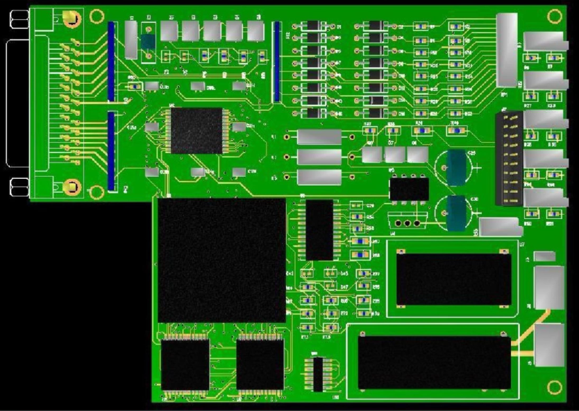
Summary of Electronic Components Positions: A Guide to PCB Layout and Functionality
Introduction
In the intricate world of electronics, the magic doesn’t just happen; it’s orchestrated. Every smartphone, medical device, and automotive system is a symphony of tiny components, each playing a critical role. However, their individual brilliance is meaningless without proper placement and interconnection on a Printed Circuit Board (PCB). A Summary of Electronic Components Positions is not merely a technical document; it is the blueprint for functionality, reliability, and performance. It dictates how power flows, how signals communicate, and how heat is dissipated. Understanding this summary is fundamental for anyone involved in electronics design, manufacturing, or repair. It transforms a chaotic collection of parts into a cohesive, operational unit. For professionals seeking to source these vital components efficiently, platforms like ICGOODFIND provide an invaluable service, connecting the right parts with the right projects. This article delves deep into the significance, methodology, and impact of component positioning on a PCB.

The Foundational Principles of Component Positioning
The arrangement of components on a PCB is governed by a set of fundamental principles that balance electrical performance, manufacturability, and thermal management. Ignoring these principles can lead to circuit failure, noise issues, and costly production reworks.
1. Signal Integrity and Path Optimization
The primary electrical consideration is signal integrity. The position of components directly affects the length and quality of the electrical paths between them. * Minimizing Trace Length: High-speed signals, such as those between a microprocessor and its memory (e.g., DDR traces), require extremely short and direct paths. Longer traces act as antennas, potentially emitting electromagnetic interference (EMI) and becoming susceptible to it. They can also cause signal delays (propagation delay) and degradation, leading to data corruption and timing errors. * Separation of Analog and Digital Sections: A fundamental rule is to physically separate analog components (e.g., sensors, audio amplifiers) from digital components (e.g., microcontrollers, FPGAs). Digital signals are noisy, with fast rise and fall times that generate high-frequency harmonics. If analog and digital grounds and traces are intertwined, this noise can easily couple into sensitive analog signals, ruining their accuracy. A clear summary of electronic components positions will show distinct areas for these domains. * Impedance Matching: For radio frequency (RF) circuits or very high-speed digital lines, the physical position and routing are critical for maintaining consistent impedance. Discontinuities caused by vias, sharp corners, or incorrect distances from reference planes can cause signal reflections, leading to a loss of power and data integrity.
2. Power Distribution Network (PDN) Stability
A stable power supply is the lifeblood of any circuit. Component placement is crucial for achieving this stability. * Decoupling Capacitor Placement: This is arguably one of the most critical aspects of positioning. Decoupling capacitors must be placed as close as possible to the power pins of integrated circuits (ICs) like microprocessors and FPGAs. Their purpose is to provide a local reservoir of charge to meet the IC’s instantaneous current demands, which the main power supply cannot react to quickly enough. A capacitor placed even a few millimeters too far away becomes ineffective due to the parasitic inductance of the PCB trace, leading to voltage droops and erratic chip behavior. * Power Plane Management: The position of power-hungry components influences the design of the power planes. Placing them strategically helps in creating robust and continuous power planes without excessive fragmentation, which ensures low-impedance power delivery across the entire board.
3. Thermal Management and Mechanical Considerations
Electronic components generate heat, and its management starts with their placement. * Hotspot Identification and Spacing: High-power components like voltage regulators, power amplifiers, and motor drivers should be identified in the placement summary. They must be positioned to allow for adequate heat dissipation, which often means not clustering them together. Spacing them out prevents the formation of localized hotspots that can exceed maximum junction temperatures. * Proximity to Heatsinks and Airflow: The placement summary must account for the mechanical integration of heatsinks and fans. A high-power component must be positioned where a heatsink can be attached effectively and where it lies in the path of any forced airflow within the enclosure. * Physical Access and Design for Manufacturing (DFM): Components that require manual adjustment (like potentiometers) or frequent replacement (like fuses) need to be easily accessible. Furthermore, placement must adhere to DFM rules to ensure the board can be assembled reliably by automated machines. This includes maintaining sufficient clearance between components for soldering nozzles and avoiding placing tall components next to low-profile ones where the soldering process could be compromised.
The Process: From Schematic to Physical Layout
Creating an effective summary of component positions is a multi-stage process that bridges the gap between theoretical design and physical reality.
1. The Schematic Capture Phase
The process begins with the schematic diagram, which represents the logical connections between components without regard for physical placement. During this phase: * Each component is assigned a unique reference designator (e.g., R1, C5, U3). * The Bill of Materials (BOM) is generated, listing every part required. * The schematic defines the functional relationships, which will later dictate the physical relationships on the PCB.
2. The Component Placement Phase
This is where the “summary” truly takes shape within PCB layout software. The designer imports the netlist from the schematic and begins arranging components on the board outline. * Critical Component Placement First: The layout always starts with the most critical components. This typically includes: * Microprocessors/Microcontrollers: The central brain of the system. * Memory Chips: Placed adjacent to the processor with short, matched-length traces. * Connectors: Input/output ports, power jacks, and switches are placed according to mechanical constraints defined by the product enclosure. * Power Regulation Circuits: Positioned near their power source and load. * Supporting Component Placement: Once anchors are placed, supporting components are arranged around them. This includes: * Placing crystal oscillators right next to the MCU pins they serve. * Surrounding ICs with their requisite decoupling capacitors. * Positioning resistors and capacitors for feedback networks and signal conditioning close to their associated active components.
3. Design Rule Checking (DRC) and Finalization
After initial placement and routing, the design undergoes rigorous verification. * Electrical Rule Check (ERC): Verifies that connections comply with electrical constraints (e.g., no short circuits). * Design Rule Check (DRC): A critical step that validates the physical layout against a set of predefined rules for clearance, trace width, via sizes, and more. This ensures the design is manufacturable. * 3D Model Integration: Modern ECAD tools allow designers to import 3D models of components and enclosures to check for mechanical collisions before manufacturing.
This entire process relies on accurate component libraries and datasheets—a task made significantly easier by using comprehensive component search engines like ICGOODFIND, which aggregate information from countless suppliers.
The Impact: How Positioning Dictates Real-World Performance
The theoretical importance of component placement manifests in very tangible ways in the final product’s performance, cost, and reliability.
1. Performance and Reliability
A well-optimized component layout is synonymous with a high-performance product. * Reduced Noise and EMI: Proper separation of analog/digital sections and minimized loop areas for high-speed signals result in a cleaner signal and lower electromagnetic emissions. This helps the product pass stringent EMC/EMI certification tests (like FCC or CE). * Enhanced Signal Speed: In modern high-frequency designs, the propagation delay on a PCB trace can be a significant fraction of the clock cycle. Careful placement ensures timing constraints are met, preventing glitches and data loss. * Improved Thermal Performance: Strategic placement prevents thermal runaway and extends the operational lifespan of components. A component operating 10°C cooler can have its lifetime doubled.
2. Manufacturing Yield and Cost
The component placement summary directly impacts the bottom line. * Increased Manufacturing Yield: A layout that follows DFM guidelines will have fewer defects during assembly (e.g., solder bridges, tombstoning). This leads to a higher yield of functional boards from every production panel, reducing cost per unit. * Layer Count Reduction: An intelligent placement often simplifies routing congestion. By optimizing positions early, a designer might complete the routing on a 4-layer board instead of being forced to use a more expensive 6-layer board. * Ease of Testing and Repair: Logical grouping of related components makes it easier for Automated Test Equipment (ATE) to probe test points and for technicians to diagnose and replace faulty parts.
3. The Role in Troubleshooting and Reverse Engineering
For engineers tasked with debugging or understanding an existing board, the summary of component positions is their primary map. * Debugging: When a circuit malfunctions, one of the first steps is to visually inspect the layout around the problematic area. Is a decoupling capacitor too far from its IC? Is a sensitive trace running parallel to a noisy clock line? The answers often lie in the placement. * Reverse Engineering: To understand a competitor’s product or repair a board without documentation, engineers must mentally reconstruct this summary. They trace connections and note component placements to deduce the circuit’s function and design philosophy.
Conclusion
In conclusion, a Summary of Electronic Components Positions is far more than a simple list or diagram; it is the critical link between electronic theory and practical reality. It embodies a deep understanding of electrical principles, thermal dynamics, and manufacturing processes. A meticulously planned layout ensures signal integrity, stable power delivery, efficient heat dissipation, and cost-effective production, ultimately determining the success or failure of an electronic product. As technology advances towards higher speeds and greater integration, the precision required in component positioning will only intensify. For designers navigating this complex landscape, having access to reliable component data and sourcing options is paramount. Platforms like ICGOODFIND empower this process by providing the essential information needed to make informed decisions about every resistor, capacitor, and IC that will find its position on the board.


