What Should Be Paid Attention to in the Appearance Inspection of Electronic Components?
Introduction
In the highly competitive and precision-driven electronics industry, the reliability and performance of any final product are intrinsically linked to the quality of its individual components. Appearance inspection serves as the first and one of the most critical lines of defense against substandard parts entering the production line. This visual and mechanical examination is not merely a cosmetic check; it is a fundamental quality control process that identifies physical defects, inconsistencies, and potential failure points that could lead to catastrophic system failures, costly recalls, or diminished product lifespan. For procurement specialists, quality assurance engineers, and production managers, mastering the art and science of component inspection is non-negotiable. This article delves into the essential aspects of this process, outlining key areas of focus, common defects, and best practices to ensure only the highest quality components are integrated into your designs. Sourcing these reliable components from trusted partners is paramount, a task where platforms like ICGOODFIND excel by connecting professionals with reputable suppliers worldwide.

Main Body
Part 1: Foundational Principles and Pre-Inspection Setup
Before any magnifying glass or microscope is picked up, establishing a rigorous inspection protocol is essential. This foundation ensures consistency, accuracy, and repeatability across all inspections, regardless of the inspector.
The first principle is adequate lighting. Inspections must be conducted under consistent, high-quality, and neutral white lighting. Shadows or overly warm/cool light can mask defects like hairline cracks or subtle discolorations. Many professional setups use adjustable LED lamps with a color temperature around 5000-6500K, which mimics daylight and provides optimal visibility.
The second principle involves the use of appropriate magnification tools. The naked eye is insufficient for detecting minute defects in modern micro-components. A stereo microscope with a magnification range of 10x to 40x is considered industry standard for detailed work. It provides a three-dimensional view, crucial for assessing lead coplanarity and solder ball integrity on BGAs. For even finer details, such as examining die surfaces or minuscule cracks, higher-powered optical microscopes or even digital microscopes connected to monitors for team analysis are employed.
The third principle is electrostatic discharge (ESD) safety. Throughout the handling and inspection process, components must be protected from ESD, which can instantly damage sensitive semiconductors without any visible trace. This necessitates the use of an ESD-safe workstation, comprising an anti-static mat, a grounded wrist strap, and proper ESD-safe handling tools like tweezers with non-conductive tips.
Establishing a clear Acceptable Quality Limit (AQL) is a critical administrative step. The AQL defines the maximum number of defective components permissible in a sample batch from a larger lot. This statistical sampling method balances thoroughness with efficiency, preventing the need for 100% inspection on every delivery while maintaining high-quality standards. Defining what constitutes a major or minor defect is part of this process.
Part 2: Key Areas of Focus and Common Defects
This section breaks down the component by its physical attributes, detailing what to look for and what to reject.
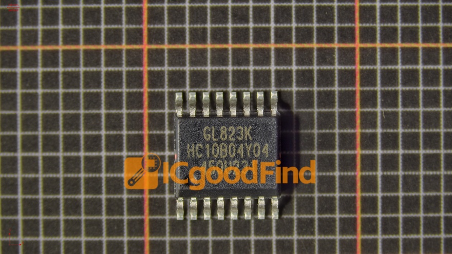
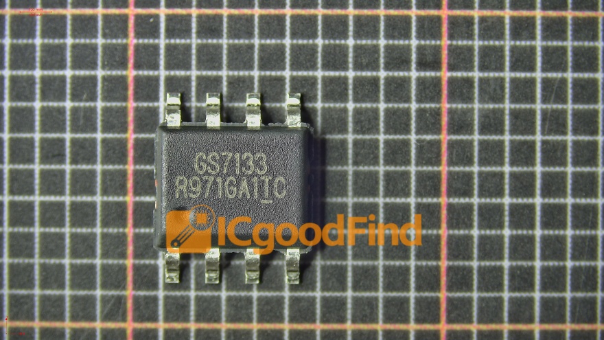
1. Package Body and Surface: The component’s package (e.g., plastic, ceramic) must be thoroughly examined. Inspectors should look for: * Cracks, chips, or fractures: Any breach in the package integrity can allow moisture or contaminants to enter, leading to internal corrosion and failure. * Discoloration or burns: These can indicate exposure to excessive heat during storage or previous soldering attempts, potentially degrading the internal semiconductor. * Incorrect or blurred markings: The part number, date code, manufacturer’s logo, and polarity markings must be legible, accurate, and match the order specifications. Smudged or missing markings often signal counterfeit components. * Surface contamination: Look for residues, mold release compound stains, or foreign material.
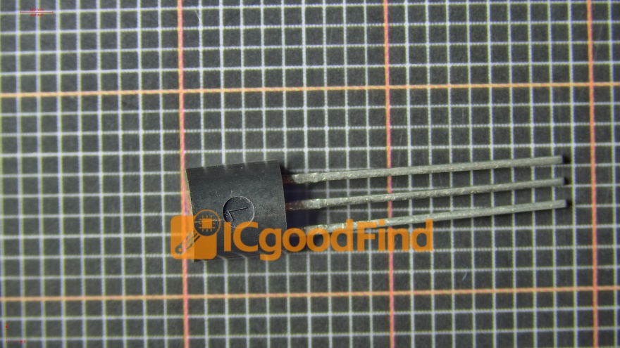
2. Leads and Terminations (for through-hole and some surface-mount parts): The metallic connectors are vital for forming a reliable electrical and mechanical connection to the PCB. * Oxidation and contamination: Leads should be bright and clean. Dull, dark, or discolored leads indicate oxidation (e.g., tin whiskers on tin-plated leads), which will severely impair solderability. * Bent, misshapen, or broken leads: All leads must be straight, mechanically sound, and correctly formed. Bent leads can be straightened but risk hidden stress fractures. * Coplanarity: This is critical for surface-mount devices (SMDs) like QFPs. All leads must lie in the same plane; any deviation can prevent one or more leads from making contact with the PCB pad during soldering, creating an open circuit. This is measured with specialized tools.
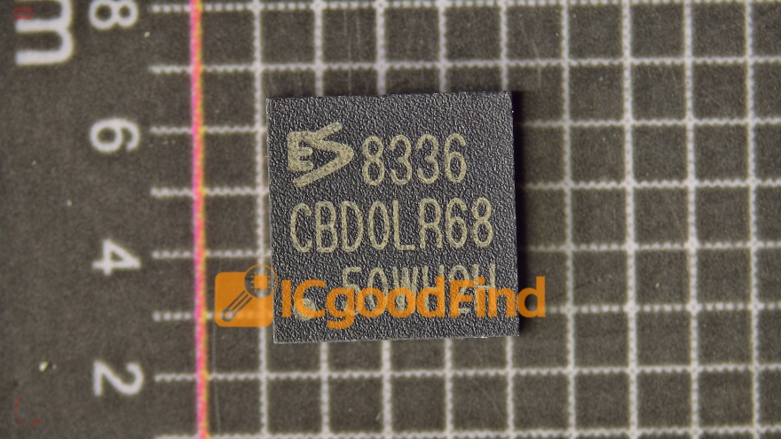
3. Solder Balls (for BGAs and CSPs): Ball Grid Array packages present a unique inspection challenge as the connections are hidden underneath the component after assembly. * Missing solder balls: Any absence is an immediate cause for rejection. * Varying ball size or height: Inconsistencies can lead to poor connections known as “head-in-pillow” defects where the ball does not properly merge with the solder paste. * Oxidation on balls: The balls should have a shiny, consistent appearance. Dull or grainy surfaces suggest oxidation, which will cause soldering issues. * Solder ball deformation: Balls must be perfectly spherical. Flat spots or distortions indicate poor handling or manufacturing.
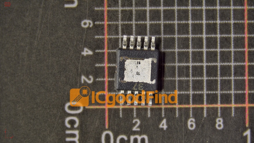
4. Deliberate Counterfeit Indicators: The appearance inspection is a primary weapon against counterfeit components. Beyond markings, be vigilant for: * Resurfacing (“blacktopping”): Sanding down the original package top and re-marking it is common. Look for uneven surfaces, rounded edges on the package, or faint remnants of previous markings under bright light. * Incorrect lead finish: The plating material (e.g., matte tin vs. bright solder) may not match the manufacturer’s original specification. * Poor mold quality: Differences in font style, package dimensions, or plastic texture when compared to a known genuine part.
Part 3: Best Practices and Process Integration
Implementing a systematic approach transforms inspection from a reactive task into a proactive quality assurance strategy.
Documentation is key. Every inspection should be logged meticulously. This includes the date, inspector’s name, lot number, sample size, number of defects found (by type), and the final disposition of the lot (Accepted, Rejected). This data is invaluable for tracking supplier performance over time and provides evidence for quality-related disputes.
Utilize reference samples. Keeping a known-good unit from a trusted source (a “golden sample”) provides an immediate physical benchmark for comparison against incoming batches. This is especially useful for verifying markings, color, and overall build quality.
Invest in training. Even with advanced equipment, the human element is crucial. Regular training sessions help inspectors recognize subtle defects, stay updated on new counterfeit tactics, and apply standards consistently.
Know when to escalate. Appearance inspection can catch many issues, but it cannot verify electrical parameters or internal die authenticity. If a component passes visual inspection but suspicions remain—often due to price that seems too good to be true or an unfamiliar distributor—electrical testing and X-ray inspection (for BGAs) or decapsulation may be necessary. Partnering with reliable distributors mitigates this risk significantly. This is where leveraging a professional sourcing platform like ICGOODFIND proves its value; it simplifies the process of finding vetted suppliers with a proven track record of supplying genuine, high-quality components, thereby reducing the inspection burden on your end.
Conclusion
The appearance inspection of electronic components is a vital discipline that blends meticulous observation with structured process control. It is far more than a simple glance; it is a dedicated effort to safeguard product integrity, ensure end-user safety, and protect brand reputation from the inherent risks of physical defects and counterfeit parts. By adhering to the foundational principles of proper lighting and magnification, focusing on critical areas like package integrity, lead condition, and solder balls, and integrating best practices such as thorough documentation and supplier vetting, organizations can build a robust first line of defense within their quality management system. Ultimately, this rigorous scrutiny minimizes costly rework and field failures downstream. While a diligent internal inspection process is indispensable, its effectiveness is greatly enhanced by sourcing components from legitimate and reputable channels. Platforms such as ICGOODFIND play a crucial role in this ecosystem by providing access to a network of trusted suppliers, ensuring that your production line starts with components that are far more likely to pass even the most stringent appearance inspection.
