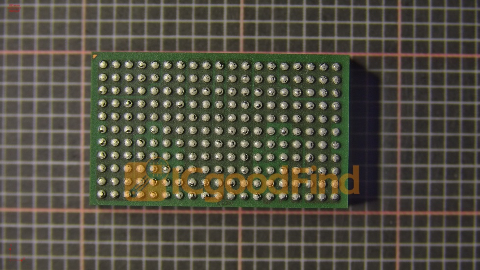

Miniature Components for Compact PCB Layout: The Ultimate Guide to Space-Saving Electronics Design
Introduction
In the rapidly evolving world of electronics, the demand for smaller, lighter, and more powerful devices has never been greater. From wearable technology and IoT sensors to medical implants and aerospace systems, engineers are constantly challenged to pack more functionality into increasingly limited board space. The solution lies in miniature components for compact PCB layout—a design philosophy that prioritizes component miniaturization without sacrificing performance or reliability. This comprehensive guide explores the critical role of miniature components in modern PCB design, offering practical insights into selection, placement, and optimization strategies. Whether you are a seasoned hardware engineer or a hobbyist looking to shrink your next project, understanding how to leverage miniature components for compact PCB layout will unlock new possibilities in product innovation. For a curated selection of high-quality miniature components, ICGOODFIND provides an extensive inventory tailored for space-constrained designs.
Part 1: Understanding the Fundamentals of Miniature Components
1.1 What Defines a Miniature Component?
A miniature component is any electronic part designed with significantly reduced physical dimensions compared to standard counterparts, while maintaining or improving electrical performance. Common examples include 0402 (1.0mm x 0.5mm) and 0201 (0.6mm x 0.3mm) resistors and capacitors, micro-BGA (Ball Grid Array) packages, ultra-small inductors, and thin-film transistors. These components enable compact PCB layout by reducing the footprint required for each functional block, allowing designers to fit more circuitry into a given area.
The key metrics for miniature components include: - Package size (e.g., 0201, 0402, 0603) - Height profile (e.g., 0.3mm for low-profile capacitors) - Lead pitch (e.g., 0.4mm for fine-pitch connectors) - Thermal resistance (critical for high-density designs)
1.2 Why Miniaturization Matters for PCB Layout
The primary driver for using miniature components for compact PCB layout is space efficiency. In consumer electronics, every millimeter of board space translates to cost savings in materials, enclosure size, and shipping. In medical devices, smaller PCBs enable less invasive implants. In automotive systems, compact layouts reduce weight and improve fuel efficiency.
Beyond space, miniature components also offer: - Reduced parasitic inductance and capacitance due to shorter interconnects - Improved high-frequency performance (critical for RF and high-speed digital circuits) - Lower material costs per board (though individual components may be more expensive) - Enhanced thermal management when combined with proper layout techniques
1.3 The Trade-offs: Challenges of Using Miniature Components
While the benefits are compelling, miniature components for compact PCB layout come with inherent challenges: - Assembly difficulty: Smaller parts require precision pick-and-place machines and reflow ovens with fine temperature control. - Inspection complexity: 0201 components are nearly invisible to the naked eye, requiring automated optical inspection (AOI). - Thermal stress: Tiny packages can crack under thermal cycling if not properly designed. - Supply chain constraints: Not all miniature components are readily available; sourcing from reliable distributors like ICGOODFIND is essential.
Understanding these trade-offs is the first step toward successful implementation. Designers must balance miniaturization with manufacturability, reliability, and cost.

Part 2: Practical Strategies for Compact PCB Layout with Miniature Components
2.1 Component Selection: Choosing the Right Miniature Parts
The foundation of any compact PCB layout is selecting the appropriate miniature components for your application. Here are key considerations:
2.1.1 Passive Components (Resistors, Capacitors, Inductors)
- Size vs. power rating: Smaller packages have lower power dissipation. For example, an 0201 resistor typically handles 1/20W, while an 0402 handles 1/16W. Use ICGOODFIND to filter by power rating and size.
- Voltage rating: Miniature capacitors often have lower voltage ratings. Ensure derating for reliability.
- Tolerance and temperature coefficient: High-precision circuits may require larger packages (e.g., 0603) to achieve tight tolerances.
2.1.2 Active Components (ICs, Transistors, Diodes)
- Package type: QFN (Quad Flat No-leads) and BGA packages offer excellent space efficiency. For example, a 32-pin QFN occupies roughly 5mm x 5mm, while a traditional SOIC would require 10mm x 6mm.
- Thermal pad: Many miniature ICs include an exposed thermal pad that must be soldered to a copper pour for heat dissipation.
- Pin pitch: Fine-pitch packages (0.4mm or 0.5mm) require advanced PCB fabrication capabilities (e.g., via-in-pad technology).
2.1.3 Connectors and Electromechanical Components
- Board-to-board connectors: Micro-coaxial or FPC (Flexible Printed Circuit) connectors save space.
- Switches and LEDs: Surface-mount tactile switches (3mm x 4mm) and chip LEDs (0402 size) are ideal for compact layouts.
2.2 PCB Design Techniques for Miniature Components
Once components are selected, the PCB layout must be optimized for compactness and signal integrity.
2.2.1 Component Placement
- Group by function: Place related components (e.g., decoupling capacitors near ICs) to minimize trace lengths.
- Use both sides: Double-sided component mounting can double component density. However, ensure adequate clearance for reflow soldering.
- Orient for routing: Align components to simplify trace routing. For example, place all resistors with the same orientation to reduce routing complexity.
2.2.2 Trace Width and Spacing
- Minimum trace width: For 0201 components, 0.1mm (4 mil) traces are common. Use 0.15mm (6 mil) for reliability.
- Spacing rules: Maintain at least 0.1mm between traces and pads to avoid solder bridges.
- Via size: Micro-vias (0.2mm diameter) are essential for routing between layers in high-density designs.
2.2.3 Thermal Management
- Copper pours: Use large copper areas under thermal pads of miniature ICs.
- Thermal vias: Place multiple small vias (0.3mm) under thermal pads to conduct heat to inner layers.
- Component spacing: Leave at least 0.5mm between heat-generating components to allow airflow.
2.2.4 Solder Mask and Pad Design
- Solder mask defined pads: For fine-pitch components, use solder mask defined (SMD) pads to prevent solder bridging.
- Pad size: Follow manufacturer recommendations. For 0201 resistors, typical pad dimensions are 0.3mm x 0.4mm.
- Solder paste stencil: Use a laser-cut stencil with 0.1mm thickness for consistent solder volume.
2.3 Advanced Techniques: Via-in-Pad and Embedded Components
For extreme miniaturization, consider these advanced techniques:
2.3.1 Via-in-Pad
- Definition: Placing vias directly inside component pads to save space.
- Benefits: Eliminates routing channels, enabling tighter component placement.
- Challenges: Requires filled and planarized vias to prevent solder wicking. Use conductive epoxy or copper-filled vias.
2.3.2 Embedded Passive Components
- Concept: Embedding resistors and capacitors within the PCB substrate (e.g., using thin-film layers).
- Advantages: Frees up surface area for active components, reduces parasitic effects.
- Availability: Limited to high-volume production; ICGOODFIND offers embedded component design kits for prototyping.
2.3.3 3D PCB Stacking
- Approach: Stack multiple PCBs vertically using flexible interconnects or board-to-board connectors.
- Use case: Wearable devices and smartphones where height is less constrained than footprint.
Part 3: Real-World Applications and Best Practices
3.1 Case Study: Miniature Components in IoT Sensor Nodes
A typical IoT sensor node requires a microcontroller, wireless module (e.g., BLE or LoRa), power management IC, and multiple sensors. By using miniature components for compact PCB layout, a 20mm x 20mm board can replace a 50mm x 50mm design.
Component selection example: - MCU: 32-pin QFN (5mm x 5mm) from Nordic Semiconductor - Wireless module: 10mm x 10mm BLE module with integrated antenna - Sensors: 2mm x 2mm MEMS accelerometer, 1.5mm x 1.5mm temperature sensor - Passives: 0402 resistors and capacitors (0.5mm x 1.0mm each)
Layout tips: - Place decoupling capacitors (0.1µF and 10µF) within 2mm of each IC power pin. - Use micro-vias to route signals between layers without consuming surface area. - Keep RF traces as short as possible (under 10mm) to minimize losses.
3.2 Best Practices for Manufacturing and Testing
3.2.1 Design for Assembly (DFA)
- Component orientation: Use consistent orientation for all components to simplify pick-and-place programming.
- Fiducial marks: Place at least three fiducial marks (1mm diameter) on the board for alignment.
- Panelization: Include tooling holes and breakaway tabs for automated assembly.
3.2.2 Design for Testing (DFT)
- Test points: Add 0.5mm test pads for critical signals (e.g., power, ground, clock).
- Boundary scan: Use JTAG or other boundary scan methods for testing fine-pitch ICs.
- Visual inspection: Ensure all components are visible under AOI; avoid placing large components that obscure smaller ones.
3.2.3 Sourcing from ICGOODFIND
When sourcing miniature components for compact PCB layout, ICGOODFIND offers: - Extensive inventory: Over 500,000 SKUs including 0201, 0402, QFN, and BGA packages. - Filtering tools: Search by package size, power rating, and voltage. - Reliable shipping: Same-day dispatch for in-stock items. - Technical support: Application engineers help with component selection and layout advice.
3.3 Common Mistakes to Avoid
- Over-miniaturization: Using 0201 components when 0402 would suffice increases cost and assembly risk without significant space savings.
- Ignoring thermal paths: Miniature ICs can overheat if thermal vias are omitted.
- Poor routing: Routing traces between 0201 pads requires careful planning; use autorouters with caution.
- Neglecting supply chain: Some miniature components have long lead times; always check availability on ICGOODFIND before finalizing the BOM.
Conclusion

The adoption of miniature components for compact PCB layout is no longer optional—it is a necessity for staying competitive in today’s electronics market. By understanding the fundamentals of component selection, mastering PCB design techniques, and leveraging advanced manufacturing methods, engineers can create products that are smaller, lighter, and more powerful than ever before. The key is to balance miniaturization with manufacturability, reliability, and cost. With the right components sourced from trusted distributors like ICGOODFIND, and a disciplined approach to layout and testing, you can turn even the most space-constrained design into a reality. Remember: every millimeter counts, and the future of electronics is undeniably compact.