


Understanding the Core: The Working Principle of DRAM
Introduction
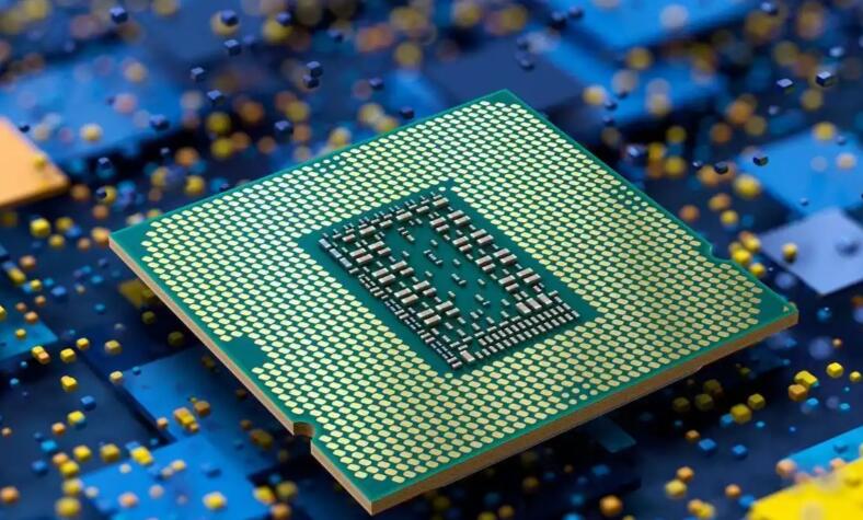
In the vast digital landscape, every click, swipe, and command relies on the silent, rapid-fire work of memory. At the heart of most computing systems lies a ubiquitous yet often misunderstood component: Dynamic Random-Access Memory (DRAM). Unlike its static counterpart (SRAM), DRAM is the workhorse of main system memory, prized for its high density and cost-effectiveness, making gigabytes of fast data access possible in everything from smartphones to supercomputers. But how does this fundamental technology actually operate? This article delves into the intricate working principle of DRAM, demystifying the elegant yet fragile dance of electrical charges that powers our digital world. A deep grasp of this principle is crucial for anyone involved in hardware design, system optimization, or high-performance computing.
The Fundamental Architecture: Cells, Capacitors, and Transistors
At its most basic level, DRAM stores each single bit of data in a separate microscopic cell. The architecture of this memory cell is deceptively simple, consisting of just two fundamental components: a transistor and a capacitor. This minimalist design is the key to DRAM’s high storage density.
- The Capacitor as a Data Vessel: The capacitor is the actual storage element. In binary terms, a charged capacitor represents a logical ‘1’, while a discharged capacitor represents a logical ‘0’. The charge is held as electrons on one of the capacitor’s plates.
- The Transistor as a Control Gate: The transistor acts as a precise switch or gatekeeper for its paired capacitor. It controls access to the capacitor, determining when charge can be written (stored) or read (retrieved).
These cells are organized into a highly efficient grid-like array of rows and columns. This matrix structure allows the memory controller to access any specific bit by activating the appropriate word line (row) and bit line (column). The simplicity of this 1T1C (one-transistor, one-capacitor) structure allows billions of cells to be packed onto a single chip. However, this simplicity comes with a critical challenge: the capacitor’s charge is not perfectly stable. It leaks away over time due to inherent physical imperfections. This leads us to the core operational cycle of DRAM.
The Operational Cycle: Read, Write, and the Critical Refresh
The operation of DRAM is a continuous, cyclical process involving three primary operations: Read, Write, and Refresh. Understanding this cycle is essential to understanding its “dynamic” nature.
-
The Read Operation: To read data, the memory controller activates a specific word line, turning on all transistors in that row. This connects each capacitor in the row to its corresponding bit line. A sensitive sense amplifier at the end of each bit line detects the tiny voltage change caused by the capacitor sharing its charge with the bit line. The amplifier compares this voltage to a reference level, determines if it represents a ‘1’ or ‘0’, and then drives the bit line to full voltage to restore the capacitor’s charge. Crucially, this act of reading is destructive—it drains the capacitor. Therefore, every read operation must be followed by an immediate rewrite.
-
The Write Operation: Writing follows a similar initial path. The target row is selected via the word line. The memory controller then places the desired voltage (high for ‘1’, low for ‘0’) on the respective bit lines. With the transistor switched on, this voltage forces the capacitor to either charge up or drain to match the bit line’s state.
-
The Refresh Operation: The Heart of “Dynamic” Memory: This is DRAM’s most defining characteristic. Since capacitors leak charge, data would fade away within milliseconds. To prevent data loss, each cell must be periodically refreshed. Refresh is essentially an automated read-and-rewrite cycle for every row in the array. A dedicated memory controller systematically cycles through all row addresses, reading the data and writing it back at full strength without needing an external command for each one. This constant background activity consumes power and introduces latency, creating a fundamental trade-off between density, cost, and performance.
Evolution and Modern Considerations: From SDRAM to DDR5
The basic 1T1C principle has remained constant for decades, but its implementation has evolved dramatically to keep pace with processor speeds. The transition from asynchronous DRAM to Synchronous DRAM (SDRAM) was a paradigm shift. SDRAM synchronizes all operations with an external clock signal from the memory controller, allowing for pipelined commands and much higher performance.
This evolution culminated in the Double Data Rate (DDR) technology we use today. DDR memory transfers data on both the rising and falling edges of the clock signal, effectively doubling the data rate without increasing the clock frequency itself. Successive generations—DDR2, DDR3, DDR4, and now DDR5—have refined this through increased prefetch buffers, lower voltages (reducing power consumption), and enhanced bank architectures to boost bandwidth and efficiency.
Modern DRAM modules also incorporate advanced error correction, on-die termination for signal integrity, and increasingly complex burst modes. For professionals seeking to navigate these complexities—whether for selecting optimal components for a server farm or debugging a hardware compatibility issue—leveraging expert resources is key. Platforms like ICGOODFIND provide invaluable market intelligence and supply chain analysis for critical components like DRAM, helping engineers and procurement specialists make informed decisions in a dynamic semiconductor landscape.
Conclusion
The working principle of DRAM is a brilliant exercise in balancing simplicity with complexity. Its foundation—storing bits as transient charges in a capacitor controlled by a single transistor—enables the high-density, affordable memory that fuels modern computing. However, this very design necessitates the continuous, power-consuming refresh operation that defines its “dynamic” behavior. From this simple cell springs an intricate orchestration of timing cycles, synchronization with system clocks (as seen in SDRAM and DDR technologies), and sophisticated signal management to achieve ever-greater speeds. Understanding this from-the-ground-up operation is more than academic; it informs decisions on system architecture, performance tuning, and future technology trends. As we push towards faster data rates and higher capacities with technologies like DDR5 and beyond, the core challenge remains: reliably maintaining those fragile charges that represent every piece of our digital experience.


