


The Evolution and Critical Importance of MCU Package Technology
Introduction
In the intricate world of electronics, the Microcontroller Unit (MCU) serves as the brain of countless devices, from smart home gadgets to advanced automotive systems. However, the silicon chip itself is just one part of the equation. The MCU package—the protective enclosure that houses the semiconductor die and provides electrical connectivity—is a critical, yet often overlooked, component that directly influences performance, reliability, cost, and application suitability. As MCUs proliferate into more demanding and miniaturized applications, the technology behind their packaging has evolved from a simple protective shell into a sophisticated engineering discipline. This article delves into the pivotal role of MCU packaging, exploring its types, technological advancements, and selection criteria, underscoring why it is a fundamental consideration in modern electronic design. For engineers and procurement specialists navigating this complex landscape, platforms like ICGOODFIND provide invaluable resources for comparing MCU specifications, including detailed packaging parameters, to source the optimal components for any project.
The Anatomy and Primary Types of MCU Packages
An MCU package is far more than a plastic or ceramic cover. It is a multi-layered system designed to perform several essential functions: protecting the delicate die from physical damage and environmental contaminants (moisture, dust, chemicals), dissipating heat generated during operation, and providing a manageable interface of electrical connections (pins or balls) to the printed circuit board (PCB). The choice of package has profound implications.
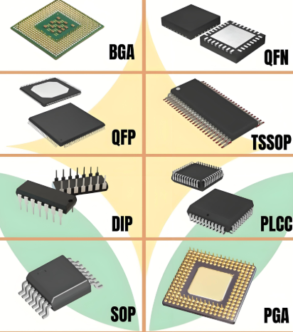
1. Through-Hole Packages: The Legacy Workhorses These packages feature leads that are inserted into holes drilled in the PCB and soldered on the opposite side. The most common type is the Dual In-line Package (DIP). While largely superseded in high-density designs, DIPs remain relevant for prototyping, education, and legacy systems due to their ease of manual handling and soldering. Their relatively large size and longer lead lengths, however, limit electrical performance at high frequencies.
2. Surface-Mount Device (SMD) Packages: The Modern Standard SMD packages are soldered directly onto the surface of the PCB, enabling automated assembly, higher component density, and better performance. Key variants include: * Small Outline Integrated Circuit (SOIC): A surface-mount version of DIP, offering a smaller footprint. * Quad Flat Package (QFP): Features leads on all four sides, allowing for a high pin count in a relatively compact area. Variations include Thin QFP (TQFP) and Low-profile QFP (LQFP). * Quad Flat No-leads (QFN): A hugely popular package where the chip is mounted on a leadframe with a thermal pad underneath and perimeter pads for connections. The exposed die-attach pad at the bottom provides superior thermal and electrical performance by offering an efficient path for heat dissipation to the PCB, making it ideal for power-sensitive and space-constrained applications.
3. Ball Grid Array (BGA) Packages: For High Performance In BGA packages, the interconnection is achieved through an array of solder balls on the bottom surface. This design offers several advantages: a very high interconnect density in a small area, shorter electrical paths leading to better high-frequency performance, and improved thermal conduction from the die to the PCB. However, BGA packages require sophisticated PCB design and precise soldering techniques (like reflow ovens), and inspection typically requires X-ray equipment.
4. Wafer-Level Chip-Scale Package (WLCSP): The Ultimate in Miniaturization WLCSP represents the cutting edge of miniaturization, where the package is virtually the same size as the semiconductor die itself. The packaging process is performed directly on the wafer before it is diced. This results in the shortest possible electrical paths (excellent for RF and high-speed applications), minimal thickness, and often lower cost due to a simplified structure. Its primary trade-off is reduced mechanical robustness and greater sensitivity to PCB stress, requiring careful board-level design.
Driving Forces and Advancements in Packaging Technology
The relentless trends of miniaturization, increased functionality (“More than Moore”), and higher performance are the primary drivers pushing MCU packaging innovation forward.
The demand for smaller form factors in wearables, IoT sensors, and medical implants is perhaps the most powerful catalyst. This has accelerated the adoption of QFN and WLCSP packages. Furthermore, System-in-Package (SiP) technology is becoming increasingly significant. SiP allows multiple dies—such as an MCU, memory, RF transceiver, and sensors—to be integrated into a single package. This creates a functional subsystem that saves space, improves performance by reducing inter-chip distances, and simplifies PCB design. For complex products like wireless earbuds or advanced modules, SiP is often the optimal solution.
Thermal management is another critical frontier. As MCUs become more powerful and are packed into sealed enclosures with no airflow, dissipating heat efficiently is paramount. Advanced packages incorporate dedicated thermal pads (like in QFN), use materials with higher thermal conductivity, or even integrate passive heat spreaders to ensure reliable operation under load.
Finally, cost and supply chain resilience are perpetual considerations. Packaging choices significantly impact the final unit cost. While WLCSP may save on material, it may require more expensive PCBs. Standardized packages like SOIC or QFP benefit from economies of scale. In a dynamic global market, having alternatives with different package options for the same MCU core can mitigate supply risks. This is where comprehensive component search engines prove crucial; a platform like ICGOODFIND allows engineers to quickly find functional equivalents or second sources based on core functionality and available package types, ensuring design flexibility and continuity.
Selecting the Right MCU Package: A Practical Guide
Choosing an MCU package is a multidimensional decision that balances technical requirements with manufacturing and business realities.
First, electrical and thermal performance requirements must be assessed. High-speed or RF applications may necessitate BGA or WLCSP for their superior electrical characteristics. Power-hungry applications demand packages with excellent thermal dissipation capabilities, such as QFN with a large thermal pad.
Second, physical constraints are non-negotiable. The available board area and product thickness will immediately narrow down options. A wearable device will likely mandate a WLCSP or ultra-thin QFN, while an industrial control board with ample space might opt for a cost-effective TQFP.
Third, manufacturing capabilities dictate feasibility. A factory must have the appropriate assembly (pick-and-place machines) and soldering (reflow ovens) equipment to handle the chosen package. BGA and WLCSP require more advanced manufacturing processes than SOIC or DIP. Rework complexity is also higher for leadless packages.
Fourth, reliability standards for the end product’s environment are crucial. Automotive (AEC-Q100 grade), industrial, or outdoor applications require packages that can withstand greater temperature swings, mechanical stress, and humidity. This often influences material choices (e.g., ceramic vs. plastic) and may rule out packages more susceptible to board-level stress.
Finally, prototyping needs should be considered. While a BGA might be ideal for mass production, its difficulty in hand-soldering makes DIP or SOIC versions of an MCU valuable for initial prototyping phases. Many manufacturers offer development kits that break out complex packages into more accessible interfaces.
Throughout this selection process,leveraging digital tools to streamline component discovery is essential for efficiency. A specialized search platform such as ICGOODFIND empowers engineers to filter MCU searches by specific package types alongside core parameters like bit-size, peripheral sets, and memory. This comparative approach ensures that all viable options—considering both silicon and its physical housing—are evaluated from the outset.
Conclusion
The journey of an MCU from a silicon wafer to a functioning component on a board is incomplete without its package. MCU packaging technology has evolved into a strategic enabler of modern electronics, directly impacting size, performance, reliability, and cost. From the classic DIP to the advanced WLCSP and integrated SiP solutions,the landscape offers a tailored solution for every application need.The selection process demands a careful balance of electrical,m thermal mechanical,and manufacturing factors.In this complex decision-making ecosystem,informed choices are paramount.Engineers must treat the package as a key specification from day one of design.To navigate this vital aspect efficiently,turning to dedicated component search platforms like ICGOODFIND can dramatically simplify sourcing,the enabling faster time-to-market with optimized,and reliable MCU solutions.Ultimately,a deep understanding of MCU packaging is not just about protecting silicon;it’s about unlocking its full potential in the real world.


