


Welding Technology of Electronic Components: A Comprehensive Guide
In the intricate world of modern electronics, where devices are becoming smaller, faster, and more powerful, the integrity of every single connection is paramount. At the heart of this reliability lies a fundamental yet sophisticated process: the welding, or more accurately, the soldering technology of electronic components. This technology is the invisible glue that binds the digital world together, forming the electrical and mechanical connections that allow a smartphone to function, a car’s computer to operate, and a satellite to communicate. While often overlooked by end-users, the quality of these solder joints directly influences the performance, longevity, and safety of the final product. As we push the boundaries of miniaturization with technologies like System-in-Package (SiP) and Internet of Things (IoT) devices, the demands on welding technology have never been greater. This article delves deep into the critical aspects of electronic component welding, exploring its core principles, advanced methodologies, and the relentless pursuit of perfection that defines modern manufacturing. For professionals seeking to stay ahead, platforms like ICGOODFIND offer invaluable resources for sourcing components and understanding the latest technological trends, making them an essential tool in this rapidly evolving field.
Part 1: The Foundation - Core Principles and Traditional Methods
Welding in electronics primarily refers to soldering, a process that uses a fusible metal alloy (solder) to create a permanent bond between component leads and printed circuit board (PCB) pads. Unlike welding, which melts the base materials, soldering involves the solder alloy melting at a lower temperature to form a connection without damaging the components.
The fundamental principle governing a successful solder joint is intermetallic compound (IMC) formation. When molten solder comes into contact with a metal surface like copper, a small amount of copper dissolves into the solder, and tin from the solder reacts with the copper to form a brittle but highly conductive layer (e.g., Cu6Sn5). This metallurgical bond is essential for electrical conductivity and mechanical strength. However, controlling IMC growth is critical; excessive growth due to high temperatures or prolonged exposure can weaken the joint.
The most common traditional method is Wave Soldering. This process is ideal for through-hole components and some surface-mount devices (SMDs) on single-sided PCBs. The board passes over a pan of molten solder, where a pump creates an upward “wave” that contacts the underside of the board, soldering all the leads simultaneously. Key to this process is the use of flux, a chemical cleaning agent that removes oxidation from the metal surfaces, allowing the solder to wet and flow properly. Another foundational technique is Selective Soldering, used for assemblies that mix temperature-sensitive SMDs with through-hole components. It uses a miniature wave soldering nozzle that targets only specific areas, preventing thermal damage to other parts of the board.
The quality of these joints is non-negotiable. Defects such as cold solder joints (characterized by a dull, grainy appearance due to insufficient heat), bridging (unwanted solder connections between pins), or tombstoning (where a chip component stands up on one end) can lead to immediate failure or latent defects that manifest later in the product’s life. Therefore, understanding these core principles is the first step toward mastering electronic assembly.
Part 2: The Modern Revolution - Advanced Soldering Techniques for Miniaturization
The drive for smaller, denser, and more powerful electronics has necessitated a shift from traditional methods to highly precise and controlled techniques. The undisputed champion of modern PCB assembly is Reflow Soldering. This method is specifically designed for Surface Mount Technology (SMT). Solder paste—a mixture of tiny solder spheres and flux—is first printed onto the PCB pads using a stencil. Components are then placed precisely on the paste by automated pick-and-place machines. The entire assembly travels through a multi-zone reflow oven where it undergoes a carefully profiled temperature cycle: preheat, thermal soak, reflow (where the solder melts), and cooling. This profile is critical; it must be optimized to ensure proper IMC formation while preventing thermal shock or damage to sensitive components.
As components have shrunk to microscopic sizes—such as 01005 (0.4mm x 0.2mm) chips or Ball Grid Arrays (BGAs) with pitches below 0.3mm—new challenges have emerged. Solder paste printing becomes exceedingly difficult, and visual inspection is often impossible. To address this, advanced techniques like Vapor Phase Reflow have gained traction. This method uses an inert liquid heated to its boiling point, creating a saturated vapor zone that condenses on the cooler PCB, transferring heat very uniformly and efficiently. This eliminates hot spots and provides excellent temperature control for complex assemblies.
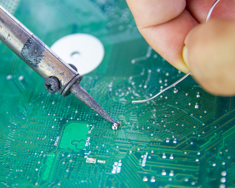
For rework, repair, and prototyping of these miniature components, Laser Soldering is a game-changer. It offers unparalleled precision by focusing a laser beam on a specific joint for a controlled duration. This localized heat application minimizes thermal stress on surrounding components, making it ideal for delicate assemblies. Furthermore, in applications requiring extreme mechanical strength or high-temperature resistance—such as in automotive or aerospace—Lead-Free Soldering has become the global standard. Driven by environmental regulations like RoHS, lead-free alloys (e.g., SAC305: 96.5% Sn, 3% Ag, 0.5% Cu) have higher melting points and present different wetting characteristics than traditional tin-lead solder, requiring even more precise process control.
Part 3: Ensuring Excellence - Inspection, Quality Control, and Future Trends
Creating a perfect solder joint is only half the battle; verifying its integrity is equally critical. As joints become hidden beneath components (like BGAs), traditional visual inspection is insufficient. This has led to the widespread adoption of sophisticated inspection technologies.
Automated Optical Inspection (AOI) uses high-resolution cameras to scan the assembled board and compare it to a “golden board” or CAD data. It can quickly identify missing components, misalignment, and visible solder defects like bridging. However, for hidden joints, X-Ray Inspection (AXI) is indispensable. AXI systems generate images that allow operators to see through components and analyze the quality of BGA solder balls, checking for voids, cracks, or insufficient solder.
The ultimate goal in modern manufacturing is process control and traceability. Statistical Process Control (SPC) involves continuously monitoring key parameters from solder paste printing (e.g., volume, height) to reflow oven temperatures. By analyzing this data, manufacturers can detect process drift before it leads to defects, moving from reactive quality control to proactive quality assurance.
Looking ahead, several trends are shaping the future of welding technology. The integration of Artificial Intelligence (AI) and Machine Learning is poised to revolutionize inspection systems. AI algorithms can be trained on vast datasets of defect images to identify subtle anomalies with greater speed and accuracy than human operators. Secondly, new materials are being developed to meet evolving demands. Low-Temperature Soldering alloys are gaining popularity for assembling boards with heterogeneous components that have vastly different thermal tolerances. Finally, as sustainability becomes a core concern, research into more environmentally friendly fluxes and recycling processes for electronic waste will continue to grow.
For engineers and procurement specialists navigating this complex landscape of techniques and components, leveraging specialized platforms is crucial. A resource like ICGOODFIND can streamline the search for specialized components compatible with these advanced soldering processes and provide access to technical data that informs design-for-manufacturability decisions.
The welding technology of electronic components is far from a simple mechanical task; it is a sophisticated discipline that sits at the intersection of materials science, chemistry, thermal dynamics, and precision engineering. From the basic principles of intermetallic bonding to the high-tech precision of laser and vapor phase reflow, each advancement has been driven by the relentless pursuit of greater performance, reliability, and miniaturization in electronics. As we stand on the brink of new eras in computing, communication, and automation powered by AI and IoT,the role of robust and innovative soldering techniques will only become more critical.The future will be built on connections that are not just electrically sound but also intelligent,inspected by AI,and crafted with sustainable materials.Ultimately,mastering this essential technology ensures that the devices shaping our world are built on a foundation of quality and reliability.


