Technical parameters/number of pins: | 8 |
|
Technical parameters/polarity: | NPN, PNP |
|
Technical parameters/dissipated power: | 2.3 W |
|
Technical parameters/breakdown voltage (collector emitter): | 60 V |
|
Technical parameters/Maximum allowable collector current: | 6.7A/5.9A |
|
Technical parameters/DC current gain (hFE): | 300 |
|
Technical parameters/operating temperature (Max): | 150 ℃ |
|
Technical parameters/operating temperature (Min): | -55 ℃ |
|
Technical parameters/dissipated power (Max): | 2.3 W |
|
Encapsulation parameters/installation method: | Surface Mount |
|
Package parameters/number of pins: | 8 |
|
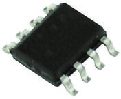
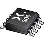
Encapsulation parameters/Encapsulation: | SOIC |
|
Dimensions/Length: | 5 mm |
|
Dimensions/Width: | 4 mm |
|
Dimensions/Height: | 1.75 mm |
|
Dimensions/Packaging: | SOIC |
|
Other/Product Lifecycle: | Unknown |
|
Other/Packaging Methods: | Cut Tape (CT) |
|
Other/Manufacturing Applications: | Power Management |
|
Compliant with standards/RoHS standards: | RoHS Compliant |
|
Compliant with the REACH SVHC standard: | No SVHC |
|
Compliant with standard/REACH SVHC version: | 2015/12/17 |
|
| Model | Brand | Similarity | Encapsulation | Introduction | Data manual | |
|---|---|---|---|---|---|---|
 PBSS4041SPN
|
NXP | 类似代替 | SOIC |
低饱和电压双 NPN/PNP 晶体管,Nexperia 一系列 NXP BISS(小信号的重大突破)低饱和电压双 NPN/PNP 双极结点晶体管。 这些设备具有极低集电极-发射极饱和电压和高集电极电流容量,采用紧凑的空间节省型封装。 这些晶体管减少损失,可在用于切换和数字应用时减少热量的产生并整体提高效率。 ### 双极晶体管,Nexperia
|
||
 PBSS4041SPN,115
|
Nexperia | 功能相似 | SOT-96-1 |
NXP PBSS4041SPN,115 双极晶体管阵列, NPN, PNP, 60 V, 2.3 W, 6.7 A, 500 hFE, SOIC
|
||
 PBSS4041SPN,115
|
NXP | 功能相似 | SOT-96-1 |
NXP PBSS4041SPN,115 双极晶体管阵列, NPN, PNP, 60 V, 2.3 W, 6.7 A, 500 hFE, SOIC
|


©Copyright 2013-2025 ICGOODFIND (Shenzhen) Electronics Technology Co., Ltd.


The most helpful review