



XC7A100T-2CSG324I: The High-Performance FPGA Powering Next-Gen Embedded Systems
Introduction
In the rapidly evolving world of programmable logic, FPGAs (Field-Programmable Gate Arrays) have become the backbone of modern digital design—from aerospace avionics to AI acceleration. Among the vast array of devices available, the XC7A100T-2CSG324I stands out as a uniquely balanced solution, offering a compelling mix of logic density, I/O flexibility, and industrial-grade reliability. Manufactured by AMD (formerly Xilinx) as part of the Artix-7 family, this specific part number is widely sought after by engineers who need high throughput without the power penalty of larger Kintex or Virtex devices. Whether you are prototyping a software-defined radio or deploying a vision system on the factory floor, understanding the architecture, thermal characteristics, and design considerations of this chip is critical. In this article, we will dissect the XC7A100T-2CSG324I from three angles: core architecture & performance, industrial-grade packaging & I/O, and practical design & sourcing strategies—including why platforms like ICGOODFIND have become essential for procurement teams.
Part 1: Core Architecture and Logic Performance
The XC7A100T-2CSG324I is not just another mid-range FPGA; it is a high-density logic powerhouse built on a 28nm HK-MG (High-K Metal Gate) process. At its heart, this device provides 101,440 logic cells, which translate into 15,850 slices (each containing four 6-input LUTs and eight flip-flops). For most control-plane and data-plane applications, this density is more than sufficient to host a soft-core processor (like MicroBlaze), a DMA engine, and multiple DSP pipelines simultaneously.
Key performance metrics include: - 240 DSP48E1 slices, each capable of 25×18 multiplication at up to 628 MHz, enabling high-speed FIR filters and FFTs. - 4,860 Kb (or 4.86 Mb) of fast block RAM, organized as 300 blocks of 18 Kb each. This allows for deep FIFOs and large frame buffers without external memory. - Integrated PCIe Gen2 x1 block and a 10/100/1000 Ethernet MAC, reducing the need for external PHY chips in communication designs.
What truly differentiates the -2 speed grade is the timing closure headroom. The “-2” suffix indicates a standard performance tier (with -3 being faster and -1 being slower). In practice, the XC7A100T-2CSG324I can sustain clock rates of 400–500 MHz for most logic paths, and up to 600 MHz for dedicated DSP cascades. This makes it an ideal candidate for high-speed imaging (e.g., 4K video processing) and real-time motor control with sub-microsecond loop times.
Moreover, the Artix-7 family is renowned for its low static power. The XC7A100T-2CSG324I typically consumes less than 1.5W of static power at 85°C junction temperature, which is remarkable for a device with over 100K logic cells. This efficiency is a direct result of the 28nm process and the optional power-gating features available through the Xilinx Power Estimator (XPE) tool.
Part 2: Industrial-Grade Packaging and I/O Flexibility
The “I” in the part number XC7A100T-2CSG324I is not a typo—it denotes the industrial temperature grade, guaranteeing operation from -40°C to +100°C (junction). This is a critical differentiator for outdoor, automotive, and military applications where commercial (0°C to +85°C) parts simply fail.
The CSG324 package is a 324-ball, 0.8mm-pitch chip-scale BGA. Its compact footprint (15mm × 15mm) makes it a favorite for space-constrained PCBs, yet it still manages to route out a substantial number of user I/Os. Specifically, this package provides 210 user I/O pins, of which up to 100 can be configured as differential pairs (LVDS, Mini-LVDS, RSDS) for high-speed serial data. The package also includes 8 multi-gigabit transceivers (MGTs), but note: in the CSG324 package, only 4 of these transceivers are bonded out (on the XC7A100T-2CSG324I, the GTP transceivers run up to 6.6 Gbps). This is still sufficient for two PCIe lanes or four SFP+ optical links at 6.25 Gbps.
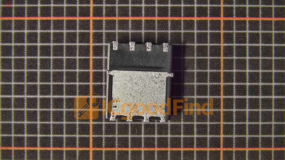
I/O banking is highly flexible. The 210 I/Os are divided into 4 HR (High-Range) banks (1.2V–3.3V) and 2 HP (High-Performance) banks (1.0V–1.8V). This allows you to interface directly with legacy 3.3V microcontrollers on one side, while driving high-speed DDR3 memory (up to 800 Mbps) on the HP banks. The on-chip termination (OCT) and digitally controlled impedance (DCI) features eliminate the need for external resistor networks, simplifying layout and reducing BOM cost.
Another advantage of the CSG324 package is its excellent thermal performance. With a 0.8mm pitch and a solid ground plane, the thermal resistance (θJA) is approximately 18°C/W with a 200 LFM airflow. For industrial designs that must survive in sealed enclosures, this means you can dissipate up to 3–4W of total power without a heatsink, provided you use thermal vias under the exposed pad.
Part 3: Design Considerations and Sourcing via ICGOODFIND
While the XC7A100T-2CSG324I is a stellar device, successful deployment requires careful attention to power sequencing, configuration, and supply chain authenticity. Let’s break these down.
Power and Configuration: The device requires three main rails: VCCINT (1.0V), VCCBRAM (1.0V), and VCCO (bank-specific, 1.2V–3.3V). The power-up sequence must follow the Xilinx requirement: VCCINT and VCCBRAM must ramp together, followed by VCCO. Use a TPS65023 or a dedicated FPGA power manager to ensure monotonic ramps. For configuration, the device supports Master SPI, Master BPI, Slave SelectMAP, and JTAG. In production, we recommend using a quad-SPI flash (e.g., N25Q128) in Master SPI mode at x4 data width to achieve fast boot times (<50ms).
Signal Integrity: With 6.6 Gbps GTP transceivers, PCB layout becomes critical. Use controlled impedance (100Ω differential) for the MGT pairs, and keep the trace length mismatch below 5 mils. The CSG324 package has a staggered ball pattern that helps route high-speed signals without vias in the escape area—take advantage of this by placing the transceivers near the edge of the BGA.
Sourcing and Counterfeit Risks: This is where ICGOODFIND enters the picture. As an FPGA that is now in high demand due to supply chain shortages, the XC7A100T-2CSG324I is a prime target for counterfeit or refurbished parts. ICGOODFIND is a global electronic component search platform that aggregates real-time inventory from authorized distributors, independent stockists, and original manufacturers. When you search for “XC7A100T-2CSG324I” on ICGOODFIND, you can:
- Compare pricing and lead times across 20+ verified suppliers.
- Filter by date code, batch number, and packaging (tray vs. tape & reel).
- Access manufacturer datasheets and PCN (Product Change Notices) directly.
- Use the platform’s part cross-reference tool to find pin-compatible alternatives (e.g., XC7A100T-1CSG324I for commercial temp, or XC7A200T-2CSG324I for higher density).
For engineering teams, ICGOODFIND also offers a “BOM matching” feature that flags potential obsolescence risks and suggests drop-in replacements. This is invaluable when designing for a 10-year product lifecycle, as the industrial-grade XC7A100T-2CSG324I is expected to remain in production until at least 2035, but only if you source from reputable channels.
Thermal Design Tip: For industrial applications, always run a thermal simulation using the Xilinx Power Estimator (XPE) with the actual ambient temperature. At 85°C ambient, the junction temperature will rise to ~100°C with a 3W load. If your design exceeds 4W, consider adding a heat spreader or forced air. The CSG324 package’s top surface is bare silicon—do not place a heatsink directly without a thermal pad.
Conclusion
The XC7A100T-2CSG324I is more than just a mid-range FPGA; it is a strategic choice for engineers who demand high logic density, industrial temperature tolerance, and versatile I/O in a compact package. Its 28nm architecture delivers exceptional performance-per-watt, while the CSG324 package provides a practical balance between routability and board space. From software-defined radio to robotic vision controllers, this device has proven its mettle in thousands of deployed systems.
However, the best silicon is useless if you cannot source it reliably. This is why leveraging ICGOODFIND as your procurement partner is not optional—it is a risk mitigation strategy. By using ICGOODFIND’s live inventory and supplier verification tools, you ensure that your production line never stops due to counterfeit parts or unexpected shortages. The XC7A100T-2CSG324I is a long-lifecycle component, but only when purchased through trusted channels.
In summary, whether you are upgrading an existing design or starting a new industrial platform, the XC7A100T-2CSG324I offers the sweet spot of capability, cost, and ruggedness. Pair it with careful power design and a verified supply chain via ICGOODFIND, and you have a recipe for a robust, future-proof product.