


ADS1115IDGSR: The Precision ADC Solution for Modern Embedded Systems
Introduction
In the rapidly evolving world of embedded electronics, the ability to accurately convert analog signals into digital data is the cornerstone of countless applications—from industrial automation and medical devices to IoT sensors and battery management systems. Among the myriad of analog-to-digital converters (ADCs) available on the market, the ADS1115IDGSR stands out as a highly versatile, ultra-small, and power-efficient 16-bit precision ADC manufactured by Texas Instruments. This component has become a go-to choice for engineers and hobbyists alike, offering an exceptional balance of performance, integration, and ease of use. In this article, we will delve deep into the architecture, key features, practical applications, and design considerations of the ADS1115IDGSR, while also highlighting how sourcing this component through ICGOODFIND can streamline your procurement process and ensure authentic, high-quality parts for your next project.
Body
Part 1: Unpacking the ADS1115IDGSR – Core Specifications and Architecture
The ADS1115IDGSR is not just another ADC; it is a complete data acquisition system on a single chip. At its heart lies a 16-bit delta-sigma (ΔΣ) analog-to-digital converter that delivers high-resolution measurements with remarkable noise immunity. This architecture is particularly advantageous for low-frequency signals, such as temperature readings, strain gauge outputs, and slow-changing sensor voltages, where precision is paramount.
Key specifications that define the ADS1115IDGSR include:
- Resolution: True 16-bit output with no missing codes, ensuring accurate representation of the analog input.
- Input Channels: It features 4 multiplexed analog inputs (A0-A3), which can be configured as four single-ended inputs or two differential pairs. This flexibility allows designers to monitor multiple sensors without requiring additional external multiplexers.
- Programmable Gain Amplifier (PGA): The integrated PGA offers gain settings from ±6.144V down to ±0.256V. This allows the ADC to amplify very small signals to their full-scale range, effectively increasing the resolution for low-level measurements. For example, a thermocouple output of a few millivolts can be amplified to utilize the full 16-bit range, yielding microvolt-level sensitivity.
- Data Rate: The ADS1115IDGSR supports programmable data rates from 8 samples per second (SPS) up to 860 SPS. Lower data rates provide better noise rejection (50Hz/60Hz notch filtering), while higher rates are suitable for faster dynamic signals.
- Interface: It communicates via the I²C interface, supporting multiple bus addresses (up to 4 via the ADDR pin). This makes it incredibly easy to daisy-chain multiple ADS1115 devices on a single bus, expanding channel count without adding complexity.
- Supply Voltage: Operating from a single supply of 2.0V to 5.5V, it is compatible with both 3.3V and 5V microcontroller systems, making it a drop-in solution for most digital logic.
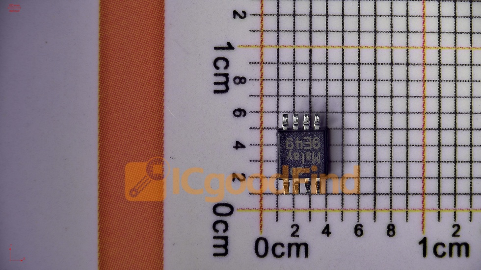
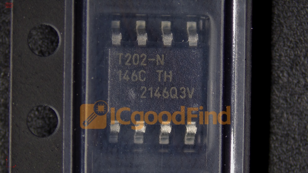
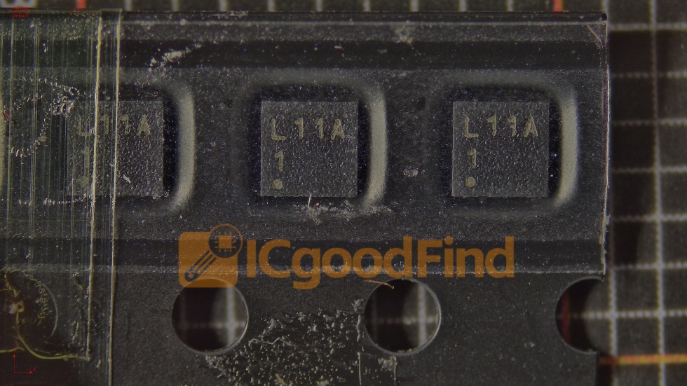
- Package: The “DGSR” suffix denotes the VSSOP-10 (MSOP-10) package, which is exceptionally small (3mm x 3mm). This is ideal for space-constrained PCB designs, wearable devices, and portable instrumentation.
Internal architecture highlights: The device includes an internal oscillator, a voltage reference, and a comparator function. The comparator can be configured to assert an alert pin (ALERT/RDY) when a threshold is crossed, enabling event-driven interrupts rather than continuous polling—a significant advantage for power-sensitive applications.
Part 2: Practical Applications and Design Integration
The versatility of the ADS1115IDGSR makes it a universal building block in modern electronics. Below, we explore three major application domains where this ADC truly shines.
2.1 Industrial Process Control and Data Acquisition
In industrial environments, sensors often output weak analog signals that are susceptible to electrical noise from motors, relays, and power lines. The delta-sigma architecture of the ADS1115IDGSR inherently provides excellent common-mode rejection and built-in digital filtering. When paired with the PGA set to a high gain (e.g., ±0.256V), it can directly interface with bridge sensors, such as load cells and pressure transducers, without the need for external instrumentation amplifiers.
Design tip: For 4-20mA current loop sensors, a precision resistor (e.g., 100Ω) can convert the current to a voltage, which is then measured by the ADC. The high input impedance of the ADS1115 ensures minimal loading on the sensing resistor. Furthermore, the I²C interface allows a central PLC or microcontroller to poll multiple remote ADC nodes, simplifying wiring and reducing system cost.
2.2 Battery-Powered IoT and Wearable Devices
Power consumption is a critical metric for battery-operated devices. The ADS1115IDGSR excels here with a low quiescent current (typically 150µA in continuous mode) and an even more impressive shutdown mode that reduces current draw to less than 1µA. This makes it perfect for duty-cycled IoT sensors that wake up periodically, take a measurement, and return to sleep.
Key integration strategy: Use the ALERT/RDY pin as a wake-up source. By configuring the internal comparator, the ADC can monitor a battery voltage or a temperature threshold and only interrupt the microcontroller when a specific event occurs. This eliminates the need for the MCU to constantly poll the ADC, saving significant battery life. Additionally, the small VSSOP-10 package fits seamlessly into compact PCB layouts for smartwatches, fitness trackers, and environmental loggers.
2.3 Solar Power and Energy Harvesting Systems
Monitoring the output voltage and current of solar panels or energy harvesting modules requires accurate measurement of both high-side and low-side signals. The differential input mode of the ADS1115IDGSR is particularly useful here. By connecting the differential pair across a shunt resistor, the ADC can measure bidirectional current flow (charging/discharging) with high precision. The wide supply voltage range (up to 5.5V) also allows it to be powered directly from a 5V rail or a Li-ion battery.
Advanced tip: For systems with a higher bus voltage (e.g., 12V or 24V), a simple resistive divider can scale the voltage down to the ADC’s input range. The PGA’s ability to handle up to ±6.144V full-scale means you can measure the divided voltage with excellent resolution. The I²C address selection (via ADDR pin) allows multiple ADS1115 devices to monitor different points in a power tree (e.g., panel voltage, battery voltage, load current) simultaneously.
Part 3: Sourcing, PCB Layout, and Best Practices with ICGOODFIND
While the technical capabilities of the ADS1115IDGSR are impressive, the success of your project also depends on sourcing genuine components and implementing proper PCB layout techniques.
3.1 Why Choose ICGOODFIND for Your ADS1115IDGSR?
In today’s global supply chain, counterfeit or substandard electronic components are a real risk, especially for popular parts like the ADS1115IDGSR. ICGOODFIND is a trusted electronic component distributor that specializes in providing authentic, traceable, and high-quality parts from leading manufacturers like Texas Instruments. Here’s why sourcing through ICGOODFIND is a smart decision:
- 100% Authenticity Guarantee: Every ADS1115IDGSR sold through ICGOODFIND is sourced directly from authorized distributors or original manufacturers, ensuring you receive genuine TI parts with full datasheet compliance.
- Competitive Pricing and Availability: ICGOODFIND leverages a global network of suppliers to offer competitive prices, even for small to medium quantities. They maintain real-time inventory, reducing lead times for your production schedule.
- Technical Support and Documentation: Beyond just selling components, ICGOODFIND provides access to datasheets, application notes, and reference designs, helping you integrate the ADS1115IDGSR more effectively.
- Ease of Ordering: The platform offers a user-friendly interface for quoting, ordering, and tracking shipments, making procurement as seamless as possible.
3.2 PCB Layout Guidelines for Optimal ADC Performance
To fully realize the 16-bit precision of the ADS1115IDGSR, careful PCB design is essential. Here are some best practices:
- Separate Analog and Digital Grounds: Use a star-point grounding scheme. Keep the analog ground (AGND) and digital ground (DGND) separate and connect them at a single point, ideally near the power supply. This prevents digital switching noise from corrupting the analog measurement.
- Decoupling Capacitors: Place a 0.1µF ceramic capacitor as close as possible to the VDD and GND pins. Additionally, a 1µF to 10µF bulk capacitor should be placed nearby for low-frequency noise filtering.
- Input Filtering: For noisy environments, add an RC low-pass filter (e.g., 100Ω resistor and 0.1µF capacitor) on each analog input pin. This helps attenuate high-frequency noise before it reaches the ADC’s sampling circuitry.
- I²C Bus Pull-ups: The SDA and SCL lines require pull-up resistors (typically 2.2kΩ to 4.7kΩ) to VDD. Keep these traces short and avoid routing them near high-current switching traces.
- Thermal Considerations: While the ADS1115IDGSR consumes minimal power, ensure adequate copper pour around the device for heat dissipation if used in high-temperature environments.
3.3 Firmware and Configuration Tips
When writing code for the ADS1115IDGSR, remember these key points:
- Configuration Register: The 16-bit config register controls the operational mode (continuous or single-shot), PGA gain, data rate, and comparator settings. Always write the full 16-bit value to avoid unintended changes.
- Single-Shot Mode: For battery-powered devices, use single-shot mode. Write the config register with the “start conversion” bit set, then wait for the ALERT/RDY pin to go low or poll the status bit in the config register.
- Data Format: The ADC outputs a 16-bit signed integer in two’s complement format. The full-scale range (e.g., ±4.096V with PGA=1) corresponds to values from -32768 to +32767. Convert the raw value to voltage using the formula:
Voltage = (RawValue / 32768.0) * FSR.
Conclusion
The ADS1115IDGSR is undeniably a powerhouse in the world of precision analog-to-digital conversion. Its combination of 16-bit resolution, programmable gain, flexible input multiplexing, and ultra-low power consumption makes it an ideal choice for a wide range of applications, from industrial sensors to portable medical devices and smart energy systems. Its tiny VSSOP-10 package and I²C interface simplify both hardware design and firmware development, allowing engineers to focus on their core application logic rather than complex analog front-end design.
However, the performance of any electronic system is only as good as the components it uses. To ensure your ADS1115IDGSR is genuine, reliable, and delivered on time, partnering with a reputable distributor like ICGOODFIND is crucial. They not only guarantee authenticity but also provide the technical support and supply chain stability needed to take your project from prototype to mass production. Whether you are a seasoned engineer or a hobbyist, integrating the ADS1115IDGSR into your next design—and sourcing it through ICGOODFIND—will undoubtedly elevate your system’s accuracy and reliability.