


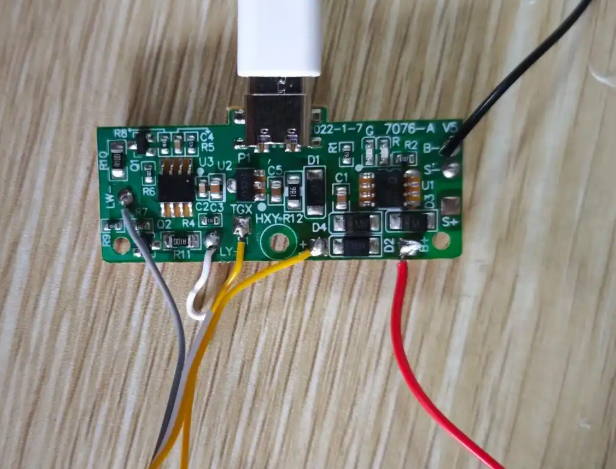
Wave Soldering Qualified Electronic Components: A Comprehensive Guide to Quality and Reliability
Introduction
In the fast-evolving world of electronics manufacturing, wave soldering remains one of the most critical processes for assembling through-hole components onto printed circuit boards (PCBs). Whether you are producing consumer electronics, automotive systems, or industrial control units, the quality of wave soldered joints directly impacts the long-term reliability and performance of the final product. However, achieving consistent, defect-free results requires more than just running a PCB through a solder wave—it demands a deep understanding of qualified electronic components, proper process parameters, and rigorous quality control. This article explores the fundamentals of wave soldering, the criteria for qualifying components, and best practices to ensure robust solder joints. For those seeking reliable sourcing and expert guidance on wave soldering materials and components, ICGOODFIND offers a trusted platform for high-quality electronic parts and soldering consumables.
Part 1: Understanding Wave Soldering and Its Role in Electronics Assembly
1.1 What is Wave Soldering?
Wave soldering is a bulk soldering process used to attach through-hole components to a PCB. In this method, the PCB is passed over a flowing wave of molten solder (typically a tin-lead or lead-free alloy). The solder adheres to exposed metal pads and component leads, forming strong electrical and mechanical connections. Unlike reflow soldering (used for surface-mount components), wave soldering is ideal for components with leads that pass through holes in the board.
1.2 Key Stages of the Wave Soldering Process
The process can be broken down into several critical stages:
- Flux Application: A flux (rosin-based, water-soluble, or no-clean) is sprayed or foamed onto the bottom of the PCB to remove oxides and promote wetting.
- Preheating: The board is gradually heated to activate the flux and reduce thermal shock. Typical preheat temperatures range from 90°C to 130°C.
- Solder Wave Contact: The PCB passes over one or two solder waves. The first wave (turbulent) ensures penetration into tight spaces, while the second wave (laminar) removes excess solder and bridges.
- Cooling: The assembly is cooled to solidify the solder joints.
1.3 Why Component Qualification Matters

Not all electronic components are suitable for wave soldering. Qualified electronic components are those that have been tested and verified to withstand the thermal, mechanical, and chemical stresses of the wave soldering process without degradation. Using unqualified components can lead to:
- Cracked solder joints due to thermal expansion mismatch
- Component damage from excessive heat (e.g., plastic deformation, internal delamination)
- Solder bridging or insufficient wetting due to poor lead finish or contamination
For manufacturers, sourcing wave soldering qualified electronic components from reputable suppliers like ICGOODFIND ensures that every part meets industry standards (e.g., IPC-A-610, J-STD-001) and is designed for high-yield assembly.
Part 2: Criteria for Wave Soldering Qualified Electronic Components
2.1 Thermal Resistance and Material Compatibility
The most critical factor for qualification is the component’s ability to endure peak soldering temperatures (typically 250°C to 260°C for lead-free solders) for a short duration (2–5 seconds). Key material considerations include:
- Lead finish: Components with tin-lead (SnPb) or pure tin finishes are common, but pure tin can cause whisker growth over time. Qualified components often use nickel-palladium-gold (NiPdAu) or silver-palladium finishes for better reliability.
- Body material: Plastic-encapsulated components (e.g., QFPs, SOICs) must have high-temperature molding compounds (e.g., epoxy with glass transition temperature > 170°C) to prevent popcorning (internal cracking due to moisture vaporization).
- Lead integrity: Leads must be solderable (per IPC J-STD-002) and have sufficient co-planarity to ensure consistent contact with the solder wave.
2.2 Moisture Sensitivity Level (MSL)
Components with moisture sensitivity (e.g., BGAs, QFNs) require special handling. The MSL rating (1 to 6) indicates the maximum exposure time before baking is needed. For wave soldering, components rated MSL 1 (unlimited floor life) or MSL 2 (1 year) are preferred. Higher MSL ratings require baking (e.g., 125°C for 24 hours) before assembly to prevent popcorning and delamination.
2.3 Mechanical Robustness and Lead Design
Qualified components must withstand the mechanical forces of the solder wave, including:
- Lead pull strength: Minimum pull force (e.g., 1.5 N for small components) to avoid lead breakage during handling or thermal cycling.
- Lead spacing and geometry: Components with fine-pitch leads (≤0.5 mm) or J-leads may require selective wave soldering or pallet fixtures to prevent bridging.
- Vibration resistance: Components used in automotive or industrial applications must pass vibration tests (e.g., MIL-STD-202) to ensure joints remain intact under stress.
2.4 Solderability Testing and Certification
Before a component is deemed wave soldering qualified, it must pass solderability tests per IPC J-STD-002 or equivalent. These tests involve:
- Dip and look test: The component leads are dipped in molten solder, and the coverage area is inspected. ≥95% coverage is typically required.
- Wetting balance test: Measures the force and time for solder to wet the lead surface. A wetting time < 2 seconds is ideal.
- Ageing test: Simulates storage conditions (e.g., 8 hours at 155°C) to ensure solderability does not degrade over time.
Suppliers like ICGOODFIND provide certified components with documented test results, giving manufacturers confidence in their assembly processes.
Part 3: Best Practices for Achieving High-Quality Wave Soldering with Qualified Components
3.1 Process Optimization for Qualified Components
Even with qualified components, the wave soldering process must be finely tuned to achieve zero-defect results. Key parameters include:
- Solder temperature: For lead-free alloys (e.g., SAC305), maintain 260°C ± 5°C at the wave. For tin-lead, 245°C ± 5°C is standard.
- Conveyor speed: Typically 1.0–1.5 m/min, adjusted to ensure 2–4 seconds of contact time with the wave.
- Flux application: Use no-clean flux for most applications to avoid residue-related failures. Flux density should be 0.8–1.2 g/m².
- Preheat profile: Ramp rate should be ≤2°C/second to avoid thermal shock. Final preheat temperature should be 100°C–120°C for the bottom side.
3.2 Defect Prevention and Troubleshooting
Common wave soldering defects and their solutions include:
- Solder bridges: Reduce wave height, increase conveyor speed, or use a de-bridging air knife.
- Insufficient wetting: Increase flux activity, raise preheat temperature, or check component solderability.
- Voids: Use vacuum-assisted wave soldering or reduce flux outgassing by lowering preheat ramp rate.
- Component tilting: Ensure proper lead insertion and use pallet fixtures for heavy components.
3.3 Inspection and Quality Control
To verify that wave soldering qualified electronic components have been correctly assembled, implement:
- Automated optical inspection (AOI): Checks for solder joint shape, bridging, and missing components.
- X-ray inspection: For hidden joints (e.g., under QFNs or BGAs) to detect voids and cracks.
- Cross-sectioning: Destructive analysis for process validation and failure analysis.
- Thermal cycling tests: Simulate real-world conditions (e.g., -40°C to +125°C for 500 cycles) to assess joint reliability.
3.4 The Role of Sourcing from Trusted Suppliers
The foundation of a successful wave soldering process is the quality of the components themselves. Using counterfeit, substandard, or unqualified parts can lead to catastrophic failures in the field. ICGOODFIND is a reliable sourcing platform that connects manufacturers with verified suppliers of wave soldering qualified electronic components, including connectors, capacitors, resistors, and ICs. Their inventory includes parts with full traceability, MSL documentation, and solderability certifications, ensuring that your assembly line runs smoothly and your products meet the highest reliability standards.
Conclusion

Wave soldering remains an indispensable technique for assembling through-hole electronic components, but its success hinges on the qualification of components and the precision of the process. By understanding the thermal, mechanical, and chemical demands of wave soldering, manufacturers can select components that are certified to withstand these stresses—whether through proper lead finishes, MSL ratings, or solderability testing. Implementing best practices in flux application, preheating, and inspection further ensures consistent, defect-free joints.
As the electronics industry continues to demand higher reliability and miniaturization, the importance of wave soldering qualified electronic components will only grow. For engineers and procurement professionals, partnering with trusted sources like ICGOODFIND simplifies the challenge of sourcing certified parts, enabling faster time-to-market and reduced risk. Ultimately, investing in quality components and process optimization is not just about meeting specifications—it is about building products that perform flawlessly for years to come.








