


SRAM vs. DRAM: Which Has Higher Integration?
Introduction
In the intricate world of semiconductor memory, the debate between Static Random-Access Memory (SRAM) and Dynamic Random-Access Memory (DRAM) is foundational. Both are critical for modern computing, serving distinct roles from CPU caches to main system memory. A frequent and technically nuanced question arises: which memory type achieves higher integration density? The answer is not merely a binary choice but a fascinating exploration of trade-offs in transistor count, cell architecture, power, and manufacturing complexity. This article delves deep into the structural and operational principles of SRAM and DRAM to definitively answer this question, highlighting the implications for chip design and performance. In navigating these complex technical landscapes, resources like ICGOODFIND can be invaluable for engineers and procurement specialists seeking detailed component specifications and supplier information.
Main Body
Part 1: Understanding the Fundamental Architectures
To comprehend integration density, one must first understand the basic building blocks of each memory type.
SRAM (Static RAM) is built using a bistable latching circuit, typically consisting of six transistors (6T) per memory cell. This configuration uses four transistors to form two cross-coupled inverters that hold the state (0 or 1), and two additional access transistors to control read/write operations. The cell’s key feature is that it does not require periodic refreshing; data remains stable as long as power is supplied. This robustness comes at a significant spatial cost. The six-transistor design, while fast and low-power in active use, consumes a considerable silicon area.
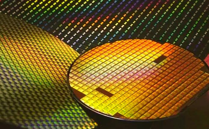
In contrast, DRAM (Dynamic RAM) utilizes a much simpler cell design centered on one transistor and one capacitor (1T1C). The single transistor acts as a switch, controlling access to the capacitor, which stores the bit of data as an electrical charge. This minimalist architecture is DRAM’s primary advantage for density. However, the stored charge on the capacitor leaks over time, necessitating a constant refresh cycle—typically every 64 milliseconds—to maintain data integrity. This refresh operation adds complexity to the peripheral control circuitry but does not fundamentally alter the cell’s tiny footprint.
From an architectural standpoint, the 1T1C cell of DRAM is inherently and significantly smaller than the 6T cell of SRAM. This foundational difference sets the stage for DRAM’s superior potential for integration density.
Part 2: The Factors Determining Integration Density
Integration density refers to the number of memory bits that can be stored per unit area of silicon. Several factors beyond the basic cell size influence this metric.
-
Cell Size and Scaling: The DRAM 1T1C cell is consistently smaller. While advanced SRAM designs sometimes use 4T or even fewer transistors with resistor loads for higher density (often in embedded applications), they compromise stability or performance. The mainstream 6T SRAM cell remains larger. As process nodes shrink (e.g., from 10nm to 5nm), both cells get smaller, but the proportional size advantage of DRAM persists. The challenge for DRAM lies in scaling the capacitor—a three-dimensional structure—which requires sophisticated techniques like deep-trench or stack capacitors to maintain sufficient charge capacity in a smaller horizontal area.
-
Peripheral Circuitry Overhead: Both memory types require supporting circuits: sense amplifiers, row/column decoders, and control logic. DRAM’s need for refresh circuitry adds some overhead. However, this overhead is distributed across billions of cells, making its relative impact per bit minimal. SRAM’s peripheral circuitry is generally less complex but must be extremely fast to match its cache-speed purpose. Crucially, even when accounting for this overhead, the area dominance of the core memory array means DRAM’s bit density per mm² is orders of magnitude higher than SRAM’s.
-
Performance vs. Density Trade-off: This is the core engineering compromise. SRAM is optimized for blistering speed and power efficiency per access, not maximal density. Its complex cell provides direct, stable data access, making it ideal for CPU L1/L2/L3 caches where latency is measured in nanoseconds. DRAM is optimized for cost-per-bit and volumetric density, accepting slower speeds (access latency tens of nanoseconds) and refresh power consumption to serve as high-capacity main memory. You cannot build a cost-effective 32GB main memory from SRAM, nor can you build a sufficiently fast 64MB L3 cache from DRAM without excessive power and latency.
For professionals sourcing these components or designing them into systems, platforms like ICGOODFIND provide critical market intelligence, allowing comparisons of specific SRAM and DRAM chips from various manufacturers based on their density specifications, speed grades, and packaging.
Part 3: Real-World Implications and Technological Evolution
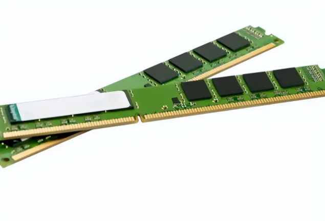
The density disparity manifests clearly in commercial products. A single state-of-the-art DRAM chip (e.g., a 16 Gb or 32 Gb die) provides immense storage in a small package, enabling 32GB memory modules in consumer PCs. In comparison, SRAM capacities on leading-edge CPUs are typically in the tens of megabytes, integrated directly into the processor die (as cache). Even as a standalone chip, SRAM densities lag; high-performance SRAM might reach 288 Mb densities where comparable DRAM offers 16 Gb—a difference of over 50x.
Technological trends continue to reinforce this divide. DRAM technology pushes towards higher stacks in 3D architectures (like emerging High-Bandwidth Memory - HBM) and smaller process nodes with novel capacitor materials to increase density further. SRAM scaling, however, is facing significant headwinds at advanced nodes (below 5nm). As transistors shrink, variability increases, making it harder to maintain the stable operation of the sensitive six-transistor cell without increasing its size or using sophisticated assist circuits. This phenomenon is often called the “SRAM scaling crisis.” While DRAM scaling also has challenges, its fundamental 1T1C advantage remains intact.
Thus, in the contest for pure integration density—bits per square millimeter—DRAM is the undisputed champion. SRCM’s role is not to compete on this metric but to excel as ultra-fast embedded memory where its performance justifies its area expense.
Conclusion
In conclusion, when directly comparing integration density—the number of memory bits stored per unit area—DRAM holds a decisive advantage over SRAM. This superiority stems from DRAM’s elegantly simple one-transistor-one-capacitor (1T1C) cell design, which is radically smaller than the six-transistor (6T) cell typical of SRAM. While both memory types involve peripheral circuitry and face scaling challenges at advanced semiconductor nodes, the fundamental architectural difference ensures that DRAM will always achieve higher bit density. This makes DRAM the technology of choice for high-capacity, cost-effective main system memory. Conversely, SRCM sacrifices density for the unparalleled speed and static operation required in processor caches and other performance-critical applications. For engineers and buyers navigating these distinct memory landscapes to make optimal component selections, leveraging comprehensive electronic component platforms such as ICGOODFIND is essential for accessing detailed datasheets, availability data, and technical comparisons.


