


The Essential Guide to DRAM Controllers: Architecture, Function, and Optimization
Introduction
In the intricate ecosystem of modern computing, memory performance is a critical bottleneck that directly impacts system speed, efficiency, and responsiveness. At the heart of this memory hierarchy lies a pivotal yet often overlooked component: the DRAM controller. Acting as the essential intermediary between a processor and the Dynamic Random-Access Memory (DRAM), the DRAM controller is the maestro orchestrating the complex symphony of data flow. Its primary role is to manage the intricate timing, scheduling, and electrical interface protocols required to read from and write to DRAM modules efficiently. As applications demand higher bandwidth and lower latency—from AI training and high-performance computing to everyday multitasking—the design and optimization of the DRAM controller have become paramount. This article delves into the architecture, core functionalities, and advanced optimization techniques of DRAM controllers, highlighting why they are a linchpin in system performance. For engineers and architects seeking cutting-edge insights into memory subsystem design, platforms like ICGOODFIND offer valuable resources and community expertise.

Part 1: Architecture and Core Components of a DRAM Controller
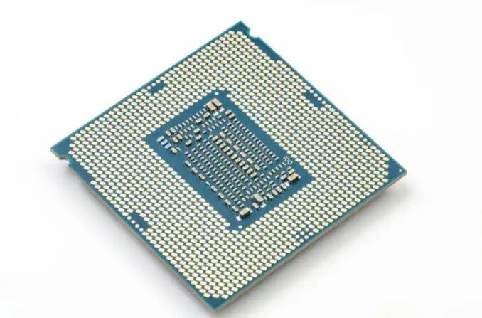
A DRAM controller is a sophisticated digital circuit, typically integrated into a processor’s memory management unit or as part of a dedicated chipset. Its architecture is designed to abstract the complex, low-level operations of DRAM from the rest of the system, presenting a cleaner interface for memory requests. The key architectural components include:
-
The Request Scheduler: This is the brain of the controller. It receives read and write commands from the CPU or other system agents via a system bus (like AMBA AXI). The scheduler’s critical job is to reorder these incoming requests to maximize efficiency. Instead of processing them in first-come-first-served order, it employs algorithms to minimize DRAM access latency and bank conflicts. It considers factors like row buffer locality (keeping an open row active) and command timing constraints.
-
The Command Generator and Timing Engine: DRAM chips require a precise sequence of commands (Activate, Read, Write, Precharge, Refresh) with strict minimum delays between them (known as tRCD, tRP, tRAS, etc.). This component translates high-level scheduler decisions into this exacting command sequence. The timing engine enforces all protocol-specific delays, ensuring the controller never violates DRAM specifications, which would lead to data corruption.
-
The Physical Layer (PHY): This component handles the electrical interface to the DRAM chips. It includes circuitry for driving signals onto the memory bus at high speeds, capturing incoming data, and performing necessary signal integrity operations like calibration (ZQ calibration) and training (read/write leveling). The PHY operates at the high-frequency clock of the memory interface (e.g., DDR4-3200) and is crucial for achieving high data transfer bandwidth.
-
The Memory Map Decoder and Address Translator: This block translates system-level physical addresses into the DRAM-specific format of bank, row, and column addresses. It understands the geometry of the installed memory modules (number of ranks, banks, rows, columns) and maps logical requests to the correct physical locations.
-
The Refresh Management Unit: DRAM cells store data in tiny capacitors that leak charge over time. To prevent data loss, each cell must be refreshed periodically (typically every 64ms). The refresh manager autonomously issues refresh commands to all banks, balancing this mandatory overhead with pending read/write operations to minimize performance impact.
Part 2: Core Functionalities and Operational Challenges
The DRAM controller’s operation is a continuous exercise in managing trade-offs between speed, power, and reliability. Its core functionalities are centered around overcoming inherent DRAM limitations.
-
Managing Latency vs. Bandwidth: A fundamental challenge is the disconnect between DRAM’s high peak bandwidth and its relatively high access latency. The initial access to a new row (row activation) is slow, but sequential accesses within that same row are fast. The controller mitigates this by employing open-page and closed-page policies. An open-page policy keeps a row active after access to exploit spatial locality, reducing latency for subsequent hits but potentially causing bank conflicts for random accesses. A closed-page policy precharges the bank immediately, optimizing for random access patterns at the cost of higher latency for sequential flows. Advanced controllers dynamically switch policies based on workload prediction.
-
Arbitration and Quality of Service (QoS): In multi-core systems or Systems-on-Chip (SoCs) with multiple masters (CPUs, GPUs, NPUs, I/O controllers), the memory controller must arbitrate between competing requests. Effective arbitration schemes ensure fair access while prioritizing latency-sensitive traffic. Implementing QoS mechanisms prevents any single agent from monopolizing memory bandwidth, which is crucial for real-time and multimedia applications.
-
Power Management: DRAM power consumption is significant. The controller implements several power-saving states (like Active Power-Down, Self-Refresh). By intelligently placing idle memory ranks or banks into low-power states during periods of low activity and quickly waking them when needed, the controller can dramatically reduce system power consumption without severely degrading performance.
-
Handling Reliability Features: Modern controllers integrate support for error-correcting code (ECC), which detects and corrects single-bit errors transparently. For higher reliability in server markets, they may also manage DRAM scrubbing (periodically reading memory to find and correct errors before they accumulate) and implement patrol scrubbing algorithms.
Part 3: Advanced Optimization Techniques and Future Trends
To push performance boundaries, contemporary DRAM controllers employ increasingly intelligent optimization techniques.
-
Advanced Scheduling Algorithms: Beyond basic First-Ready First-Come-First-Served (FR-FCFS), modern schedulers use more complex algorithms that consider thread-awareness (to reduce interference in multi-core CPUs), write-drain policies to manage the write buffer efficiently, and look-ahead scheduling to better group commands.
-
Command Overlap and Bank Parallelism: To fully utilize available bandwidth, controllers schedule commands to different banks in an overlapped fashion. While one bank is being precharged or activated, another bank can be reading or writing data. Maximizing this bank-level parallelism is key to saturating the memory bus.
-
Adaptive Controller Tuning: Machine learning is being explored to create controllers that can adapt their scheduling policy, arbitration weights, and power management parameters in real-time based on the observed workload characteristics. This moves beyond static algorithms towards self-optimizing memory subsystems.
-
Support for Emerging Memory Standards: As DDR5 becomes mainstream and standards like LPDDR5X/LPDDR6 dominate mobile and high-performance computing, controllers evolve rapidly. DDR5 introduces features like dual sub-channels (effectively doubling burst length), on-die ECC for improved reliability at higher densities, and more granular refresh commands (Same-Bank Refresh). The controller must be redesigned to leverage these features for performance gains. Staying abreast of these complex hardware design trends requires dedicated knowledge hubs. For professionals navigating these advancements, resources aggregated on platforms like ICGOODFIND can be instrumental in providing technical papers, architectural analyses, and industry discussions.

Conclusion
The DRAM controller is far more than a simple interface; it is an intelligent performance engine that dictates the efficiency of one of computing’s most critical paths: main memory access. Its sophisticated architecture—encompassing schedulers, timing engines, PHYs—works tirelessly to mask DRAM latency, maximize bandwidth, conserve power, and ensure data integrity. As computational workloads grow more demanding and memory technologies like DDR5 and beyond continue to evolve, the role of the DRAM controller will only become more central. Ongoing innovations in scheduling algorithms, adaptive machine learning-based management, and support for novel memory protocols are pushing the boundaries of what’s possible. Ultimately, a deep understanding of DRAM controller design principles is essential for anyone involved in crafting the high-performance systems of today and tomorrow.


