The Fundamental Difference Between NAND and DRAM: A Guide to Memory Technologies
Introduction
In the intricate world of digital electronics, two types of memory are fundamental to the operation of nearly every computing device: NAND flash and DRAM. While often mentioned together in discussions about storage and memory, they serve vastly different purposes. For professionals, enthusiasts, and anyone looking to optimize system performance—whether for high-end computing, data center management, or selecting components for a new device—understanding the core distinction between volatile and non-volatile memory is crucial. This article delves deep into the architectural, functional, and application-based differences between NAND and DRAM, clarifying why both are essential yet irreplaceable in modern technology. For those seeking detailed component analysis and sourcing, platforms like ICGOODFIND provide invaluable resources to compare specifications and supply chains for these critical semiconductors.
Main Body
Part 1: Architectural and Operational Principles
At their most basic level, NAND flash and DRAM are built on different physical principles and architectures, which dictate everything about their performance and use.
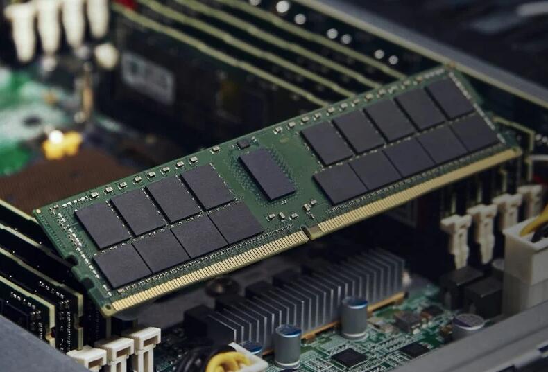
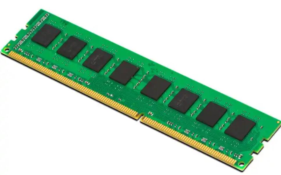
DRAM (Dynamic Random-Access Memory) is a type of volatile memory. Its basic building block is a tiny capacitor paired with a transistor, forming a memory cell. The capacitor holds an electrical charge to represent a binary ‘1’, while no charge represents a ‘0’. However, this charge leaks away over milliseconds. Therefore, DRAM requires constant power and periodic refreshing (re-reading and re-writing the data) to maintain its stored information. This “dynamic” refresh process is where it gets its name. Architecturally, DRAM cells are arranged in a simple, grid-like pattern, allowing for very fast random access to any byte of data. This speed comes at the cost of density; the capacitor-transistor pair is relatively large compared to advanced NAND cells.
NAND Flash Memory is a non-volatile storage technology. It uses floating-gate transistors as memory cells. Data is stored by trapping electrons on an insulated gate within the transistor. The presence or absence of these electrons alters the transistor’s threshold voltage, defining the stored bit. Crucially, these trapped electrons remain in place without power, making NAND “non-volatile.” NAND cells are connected in series (like a NAND logic gate), creating dense arrays. However, this architecture means data cannot be accessed at the byte level. Instead, it must be read and written in larger blocks (pages) and erased in even larger blocks (blocks). This fundamental structure leads to slower write/erase speeds and finite endurance, as the insulating layer degrades each time electrons are forced through it.
Part 2: Performance Characteristics: Speed, Endurance, and Cost
The architectural differences manifest directly in the performance profiles of each memory type, creating a clear trade-off landscape.
Speed and Latency: DRAM is significantly faster than NAND flash, especially for write operations and random access. Modern DDR4/DDR5 DRAM offers access times measured in nanoseconds (ns) and bandwidths in tens of gigabytes per second (GB/s). It acts as the system’s high-speed workspace for actively running applications and operating system processes. In contrast, even the fastest NVMe SSDs (based on NAND) have access times measured in microseconds (µs)—thousands of times slower than DRAM—for random reads, with writes being slower still. NAND excels in sequential data transfer but cannot match DRAM’s low latency.
Endurance and Persistence: This is the defining trade-off. DRAM has virtually unlimited read/write endurance but loses all data instantly when power is cut. Its volatility makes it unsuitable for long-term storage. NAND flash has a finite number of Program/Erase (P/E) cycles—anywhere from hundreds for older TLC to tens of thousands for high-end SLC cells. After this limit, cells can no longer reliably store data. However, its non-volatility makes it perfect for storing files, operating systems, and applications persistently.
Cost and Density: On a cost-per-bit basis, NAND flash is far cheaper than DRAM. This allows for massive storage capacities (terabytes) in consumer devices at reasonable prices. DRAM’s complex structure and need for speed make it more expensive per gigabyte, which is why system RAM is typically measured in gigabytes. The industry trend is to increase density for both: DRAM scales through smaller process nodes and 3D stacking techniques like TSV, while NAND has moved decisively into 3D stacking of cell layers to increase capacity without shrinking the planar cell size further.
Part 3: Primary Applications and System Synergy
NAND and DRAM are not competitors but complementary technologies that work in concert within a computing hierarchy.
DRAM’s Role: The High-Speed Working Memory. It functions as the CPU’s primary workspace. When you open a program or file, it is loaded from slow storage (like NAND) into DRAM for the processor to work on it at high speed. It holds the operating system’s kernel, application code, and active data sets. More DRAM allows a system to handle more tasks simultaneously without slowing down to fetch data from storage.
NAND’s Role: The Bulk Storage Layer. It serves as the primary medium for long-term data retention. This includes everything from your device’s firmware and operating system to documents, photos, videos, and installed applications. Its forms include SSDs (SATA & NVMe), USB flash drives, SD cards, and embedded storage in smartphones (eMMC/UFS). The rise of NAND-based SSDs over hard disk drives has been the single biggest performance upgrade for computers in recent decades.
Synergy in Modern Systems: A modern computer or smartphone uses both seamlessly. For example, when editing a large image file: the application software resides on the NAND SSD; upon launch, it’s loaded into DRAM for execution; the image file is read from SSD into DRAM for editing; changes are temporarily held in DRAM; upon saving, the modified data is written back from DRAM to the NAND SSD. Technologies like caching (using fast NVMe NAND as a cache for hard drives) and swap/virtual memory (using part of an SSD as overflow for when DRAM is full) further blur the lines but rely on their inherent differences.
Conclusion
In summary, the essential difference between NAND and DRAM lies at the intersection of volatility versus non-volatility, which dictates their speed, cost, endurance, and ultimate role within a system. DRAM is the fast, volatile workhorse for active computation, while NAND is the slower but persistent foundation for mass storage. Understanding this dichotomy is key to making informed decisions about hardware upgrades, system design, and troubleshooting performance bottlenecks. As technologies evolve with innovations like 3D XPoint (Optane) and CXL-attached memory blurring traditional boundaries, this foundational knowledge remains more important than ever. For engineers, purchasers, and tech enthusiasts needing to navigate the complex semiconductor market for these components—whether for qualification, pricing, or availability—leveraging a specialized platform like ICGOODFIND can streamline the process of finding reliable information and suppliers.