


Schematic Diagram of MCU Minimum System: A Comprehensive Guide for Engineers
Introduction
In the realm of embedded systems and electronics design, understanding the Schematic Diagram of an MCU Minimum System is a fundamental cornerstone. A Microcontroller Unit (MCU) minimum system, often called the “bare minimum” circuit, is the essential configuration required to make a microcontroller operational independently. This setup allows the MCU to execute programmed instructions without external complexities. For developers, hobbyists, and engineers, mastering this schematic is not just academic—it’s a practical necessity for prototyping, debugging, and deploying robust embedded applications. This article delves deep into the components, design principles, and best practices for creating a reliable MCU minimum system schematic. By demystifying each segment of the diagram, we aim to provide a clear roadmap for building stable microcontroller foundations. For those seeking specialized components or detailed reference designs, platforms like ICGOODFIND offer valuable resources to streamline the procurement and research process.

The Core Components of an MCU Minimum System Schematic
A typical schematic diagram for an MCU minimum system revolves around three indispensable elements: power supply, clock circuit, and reset circuit. Each plays a critical role in ensuring the microcontroller’s stability and performance.
First, the power supply section is paramount. Most MCUs operate at low voltages (e.g., 3.3V or 5V), requiring precise regulation. The schematic must include voltage regulators (like LM7805 or AMS1117), decoupling capacitors, and filtering networks. Decoupling capacitors—usually a combination of 100nF ceramic and 10µF tantalum capacitors—are placed close to the MCU’s power pins to suppress noise and provide instantaneous current during switching events. A poorly designed power supply can lead to erratic behavior, resets, or permanent damage.
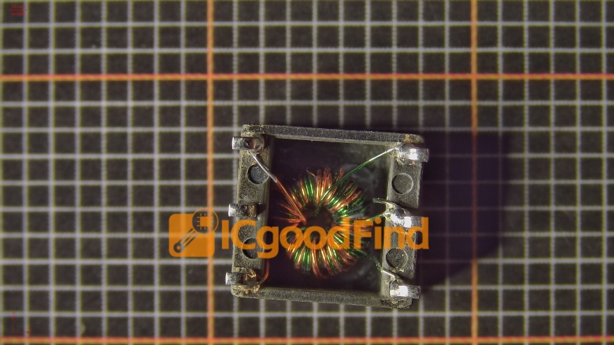
Second, the clock generation circuit provides the heartbeat for the MCU. While many modern microcontrollers feature internal oscillators, external clock circuits are often used for higher accuracy and stability. The schematic typically shows a crystal oscillator (e.g., 16MHz for ATmega328P) connected across the MCU’s XTAL pins, with two load capacitors grounding each crystal leg. Alternatively, for simpler timing needs, a ceramic resonator or an external RC network might be depicted. The choice impacts timing precision and power consumption—a key consideration in battery-powered designs.
Third, the reset circuit ensures the MCU starts in a known state. A simple manual reset can be implemented with a push-button switch connected between the RESET pin and ground, paired with a pull-up resistor to VCC. More advanced schematics might include power-on reset (POR) circuits using RC networks or dedicated reset ICs to generate a clean reset pulse during voltage fluctuations. This section is crucial for reliability; without a proper reset mechanism, the MCU may fail to initialize correctly after power-up or during brown-out conditions.
Design Principles and Layout Considerations
Creating an effective schematic goes beyond merely connecting components; it involves adhering to proven design principles and anticipating real-world challenges.
Signal integrity and noise reduction are primary concerns. In the schematic, this translates to strategic placement of ground planes, short and direct traces for high-speed signals, and adequate separation between analog and digital sections. For instance, the analog reference voltage (AVCC) pin should be isolated with ferrite beads or LC filters if shown in the diagram. Additionally, ESD protection diodes on communication lines (like UART or I/O pins exposed to connectors) are often included to safeguard against electrostatic discharge.
Minimizing power consumption is another critical principle, especially for IoT and portable devices. The schematic should facilitate low-power modes by including provisions for disabling unused peripherals and employing sleep-mode configurations. This might involve using MOSFETs to cut power to external sensors or illustrating precise connections for wake-up interrupts. Furthermore, selecting components with low quiescent current for voltage regulators directly impacts battery life.

The schematic’s clarity and documentation cannot be overstated. A well-drawn diagram uses consistent symbols, clear net labels, and functional grouping of components. It should explicitly denote test points for debugging (e.g., LED indicators on key signals) and include notes on critical tolerances (like capacitor ESR for decoupling). Tools like hierarchical design can break complex systems into manageable sheets—power supply on one sheet, clock on another—enhancing readability. For engineers sourcing parts or comparing alternatives, resources such as ICGOODFIND prove invaluable in verifying component specifications and availability directly from suppliers.
Common Pitfalls and Troubleshooting Guidance
Even with a theoretically perfect schematic, practical implementation often reveals hidden issues. Recognizing common pitfalls can save significant development time.
One frequent mistake is incorrect decoupling capacitor implementation. Designers might place capacitors too far from the MCU pins or use inappropriate values, leading to voltage droops and noise-induced errors. The schematic must specify capacitor placement adjacent to each power pair. Another oversight involves clock circuit stability; using crystals without correct load capacitance or routing clock traces near noisy lines can cause frequency drift or startup failures.
Reset-related problems are also prevalent. A reset pin left floating (without a pull-up resistor) can cause random resets due to electromagnetic interference. Similarly, ignoring the MCU’s brown-out detection (BOD) settings in the schematic—by not including necessary jumper selections or voltage divider networks—can make the system unreliable in fluctuating power environments.
Debugging a malfunctioning minimum system requires methodical checks. Start by verifying power supply voltages with a multimeter or oscilloscope to ensure they are within tolerance and free of ripple. Next, probe the clock signal to confirm its presence and frequency. A logic analyzer can help inspect reset pin behavior during power-up. If issues persist, re-examine the schematic for subtle errors like swapped pin assignments or incorrect net connections on shared buses like SPI or I2C. Sometimes, consulting reference designs from component manufacturers or platforms like ICGOODFIND can provide insights into proven layouts and alternative component choices that resolve persistent issues.
Conclusion
The Schematic Diagram of an MCU Minimum System is more than just a collection of symbols and lines—it is the blueprint for embedded system reliability and performance. By thoroughly understanding its core components (power, clock, reset), adhering to sound design principles (signal integrity, low-power optimization), and avoiding common implementation pitfalls, engineers can create robust foundations for any microcontroller-based project. A well-crafted schematic not only ensures functionality but also simplifies debugging and scaling for future enhancements.
As technology evolves with more integrated MCUs offering built-in peripherals, the minimum system concept remains vital for isolating core operational requirements from application-specific complexities. Whether you are a student building your first prototype or a professional optimizing a product design, continuous learning from reliable sources—including component databases like ICGOODFIND—is key to staying ahead in the fast-paced world of electronics design.


