


MCU Pin Diagram: The Ultimate Guide to Understanding and Utilizing Microcontroller Pinouts
Introduction
In the intricate world of embedded systems and electronics design, the Microcontroller Unit (MCU) serves as the brain of countless devices. However, even the most powerful MCU is rendered useless without a proper understanding of its interface to the external world: its pins. An MCU Pin Diagram, often referred to as a pinout, is the fundamental blueprint that maps every physical pin on the microcontroller package to its specific function. This document is not merely a technical chart; it is the essential roadmap for hardware engineers, hobbyists, and developers to connect power, communicate with peripherals, and bring their electronic designs to life. Mastering the pin diagram is the critical first step between a concept on paper and a functioning prototype on the bench. As we delve into the complexities of pin configurations, multiplexing, and power planning, resources like ICGOODFIND can be invaluable for sourcing reliable components and cross-referencing accurate technical data sheets.
Main Body
Part 1: Deciphering the MCU Pin Diagram - Symbols, Labels, and Functions
A typical MCU pin diagram can appear daunting at first glance, but it follows a logical structure. Each pin is represented with a label that defines its primary and often secondary functions.
- Power Pins (VCC, VDD, GND): These are non-negotiable connections. VCC/VDD pins supply power to the MCU’s core and I/O circuits, while GND (Ground) pins provide the essential return path. High-performance MCUs may have multiple pairs of these pins to ensure stable voltage distribution and minimize noise. Missing or improperly connecting even one power pin can lead to erratic behavior or complete failure.
- General-Purpose Input/Output (GPIO) Pins: These are the workhorses of the MCU. They can be configured by software as either digital inputs (to read a button press) or digital outputs (to drive an LED). Their flexibility is key to interfacing with simple components.
- Special Function Pins: This is where the MCU’s integrated peripherals become accessible. Key groups include:
- Analog Pins (ADC): Designated for analog-to-digital conversion, allowing the MCU to read variable voltages from sensors like potentiometers or temperature probes.
- Communication Interface Pins: These include Serial Peripheral Interface (SPI), Inter-Integrated Circuit (I2C), and Universal Asynchronous Receiver/Transmitter (UART) pins. They are critical for communicating with other chips, displays, sensors, and modules.
- Timers and PWM Pins: Pins capable of generating precise Pulse-Width Modulation (PWM) signals for controlling servo motors, LED brightness, or motor speed.
- Clock and Reset Pins: External oscillator (XTAL) pins for connecting crystals and reset (RST) pins for initializing the MCU.
Understanding that a single physical pin can serve multiple functions—a concept known as pin multiplexing—is crucial. The pin diagram will list all alternate functions (e.g., PA1: GPIO_A1 / ADC1_IN2 / TIM2_CH3), and the developer must configure internal registers to select the desired mode.
Part 2: The Critical Role of Pin Diagrams in PCB Design and System Integration
The pin diagram directly translates into the physical layout of a Printed Circuit Board (PCB). A well-planned layout based on a accurate pinout is vital for signal integrity, manufacturability, and performance.
- Schematic Capture: The pin diagram is used to create the symbolic representation of the MCU in the schematic. Each pin is connected to nets that represent wires on the PCB. Grouping related signals (e.g., all SPI signals) together in the schematic improves readability and reduces wiring errors during layout.
- PCB Layout and Routing: The physical placement of components and routing of copper traces are guided by the pinout. Strategic placement involves:
- Placing decoupling capacitors as close as possible to VCC/GND pin pairs.
- Routing high-speed communication traces (like SPI) with matched lengths and away from noisy sources.
- Ensuring adequate power trace width to handle required current.
- System-Level Planning: Before any design begins, engineers must perform “pin assignment.” This involves allocating specific pins for specific functions in the end application. Considerations include:
- Which peripherals conflict due to shared internal resources?
- Are sensitive analog inputs placed away from noisy digital GPIOs?
- Is the chosen pin capable of sourcing/sinking enough current for its connected load?
A mistake in interpreting the pin diagram at this stage can lead to a non-functional board requiring costly and time-consuming revisions.
Part 3: Advanced Considerations: Power Sequencing, Debug Interfaces, and Unused Pins
Beyond basic connections, expert use of an MCU pin diagram involves nuanced considerations that separate a working prototype from a robust product.
- Power Sequencing and Multiple Voltage Domains: Modern MCUs often have separate power pins for core logic (VDD_CORE), I/O banks (VDD_IO), and analog circuits (VDDA). The pin diagram specifies absolute maximum ratings and sometimes sequence requirements. Applying I/O voltage before core voltage, for example, can cause latch-up or excessive current draw.
- Debugging and Programming Interfaces: Pins dedicated to Serial Wire Debug (SWD) or JTAG are your gateway to in-circuit programming and debugging. These pins must be accessible on the PCB, often via a header connector, and should not be used for other functions that could interfere with the programming tool.
- Handling Unused Pins: Leaving pins unconnected (“floating”) can lead to increased power consumption or unpredictable behavior as they pick up environmental noise. The pin diagram helps identify these pins so they can be properly terminated in software (configured as output-low or input with internal pull-up/pull-down) or hardware.
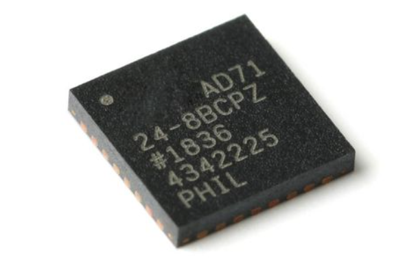
- Package Variations: An MCU comes in various packages (e.g., LQFP, QFN, BGA). The same silicon die will have different pinouts for different packages. It is imperative to reference the exact pin diagram for your specific MCU model and package type. A BGA package will have a different ball-map than an LQFP’s peripheral pinout.
For designers sourcing components or verifying specifications across different suppliers, platforms like ICGOODFIND provide a centralized resource to access and compare official datasheets—the primary source for accurate pin diagrams—ensuring design integrity from day one.
Conclusion
The MCU Pin Diagram is far more than a simple reference; it is the foundational document that bridges abstract software code and tangible hardware reality. From ensuring stable power delivery through VCC/GND pairs to harnessing advanced peripherals via multiplexed communication pins, every connection traces back to this critical map. A deep understanding of pin functionality, coupled with strategic planning for PCB layout and system integration, is paramount for successful embedded design. As projects grow in complexity, leveraging comprehensive component databases such as ICGOODFIND becomes essential for accessing reliable documentation and making informed component choices. By mastering your MCU’s pinout, you unlock its full potential and lay a solid foundation for efficient, reliable, and innovative electronic products.


