
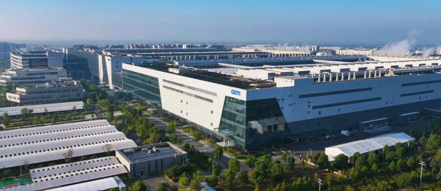


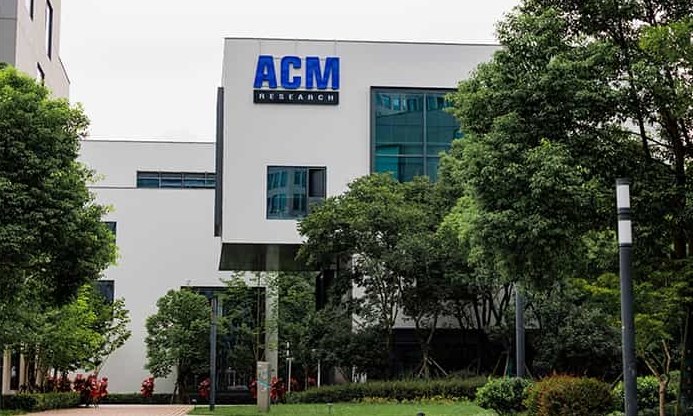
Amid a global shortage of High Bandwidth Memory (HBM), a critical component for AI computing, ACM Research (Shanghai), Inc. has announced a significant breakthrough. The company has successfully developed a suite of core equipment specifically designed for HBM fabrication and packaging, challenging the dominance of established international players.
A standout product is the company's Ultra ECP 3d electroplating tool, engineered to solve a key challenge in HBM manufacturing: copper filling for Through-Silicon Vias (TSVs). The tool achieves a high yield rate of 99.8% and supports structures for 5nm-class advanced processes and HBM's high aspect ratios. It has already entered the supply chain for a major memory maker like Samsung.
ACM Shanghai has also made comprehensive progress in the cleaning segment, crucial for HBM yield. Its SAPS and proprietary TEBO megasonic cleaning technologies enable precise, damage-free cleaning of complex HBM 3D structures, reducing leakage current by several orders of magnitude. These technologies are already deployed in production lines at industry giants, including SK Hynix and Micron.
The company's offerings extend to the packaging and testing stage. Its full line of wet processing, coating, developing, and plating equipment is adaptable for both HBM and high-performance chip 2.5D packaging. Notably, its FOPLP (Fan-out Panel Level Packaging) electroplating system, capable of handling 610x457mm large panels, meets the high-density demands of AI chips and is considered internationally competitive.
ICgoodFind's Insight
ACM Shanghai's progress in developing a full HBM process equipment portfolio marks a pivotal step for China's semiconductor supply chain independence. Securing validation from top-tier global memory manufacturers demonstrates its capability to compete in one of the most demanding and strategically vital segments of chipmaking.


