


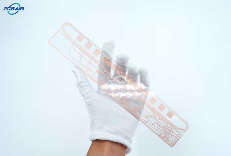
Shenzhen-based company PCBAIR has officially launched its 8-layer glass-core printed circuit board (PCB) manufacturing technology. This innovation is specifically engineered to address the critical "computing-bandwidth gap" in AI and high-performance computing (HPC), providing a novel domestic solution for advanced chip packaging.
The technology introduces several crucial benefits for large-scale, high-end chip packaging. It employs a symmetrical, low internal stress stack-up structure. Crucially, the glass core's thermal expansion coefficient is highly similar to silicon, which fundamentally reduces the risk of warping and de-soldering during large-package assembly, thereby improving reliability and production yield. On the performance front, it supports high-density interconnects with Through-Glass Vias (TGV) diameters of <20μm and Df (dissipation factor) <0.002, enabling higher I/O density and lower signal loss for demanding applications.
These features make the PCB ideally suited for the extreme requirements of AI accelerators and HPC servers. The technology provides robust support for advanced packaging approaches like Chiplet architectures and Co-Packaged Optics (CPO) that rely on high-density, low-latency interconnects.
A significant advantage for the industry is its full compatibility with existing substrate assembly lines. This design allows for rapid adoption without requiring costly equipment upgrades, significantly lowering the barrier to commercialization and accelerating the use of glass-core technology in high-end applications.
ICgoodFind's Insight
PCBAIR's breakthrough represents a tangible step forward in domestic high-end PCB capability. By directly tackling the material and signal integrity challenges of AI/HPC packaging, this glass-core technology has the potential to become a key enabler for next-generation computing hardware.


